MAX7301
Initial Power-Up
On initial power-up, all control registers are reset, and
the MAX7301 enters shutdown mode (Table 4).
Transition (Port Data Change) Detection
Port transition detection allows any combination of the
seven ports P24–P30 to be continuously monitored for
changes in their logic status (Figure 5). A detected
change is flagged on port P31, which is used as an
active-high interrupt output (INT). Note that the
MAX7301 does not identify which specific port(s)
caused the interrupt, but provides an alert that one or
more port levels have changed.
The mask register contains 7 mask bits that select
which of the seven ports, P24–P30 are to be monitored
(Table 8). Set the appropriate mask bit to enable that
port for transition detect. Clear the mask bit if transitions
on that port are to be ignored. Transition detection
works regardless of whether the port being monitored is
set to input or output, but generally it is not particularly
useful to enable transition detection for outputs.
Port P31 must be configured as an output in order to
work as the interrupt output INT when transition detec-
tion is used. Port P31 is set as output by writing bit D7
= 0 and bit D6 = 1 to the port configuration register
(Table 1).
To use transition detection, first set up the mask regis-
ter and configure port P31 as an output, as described
above. Then enable transition detection by setting the
M bit in the configuration register (Table 7). Whenever
the configuration register is written with the M bit set,
the MAX7301 updates an internal 7-bit snapshot regis-
ter, which holds the comparison copy of the logic states
of ports P24 through P30. The update action occurs
regardless of the previous state of the M bit, so that it is
not necessary to clear the M bit and then set it again to
update the snapshot register.
When the configuration register is written with the M bit
set, transition detection is enabled and remains
enabled until either the configuration register is written
with the M bit clear, or a transition is detected. The INT
output port P31 goes low, if it was not already low.
Once transition detection is enabled, the MAX7301
continuously compares the snapshot register against
the changing states of P24 through P31. If a change on
any of the monitored ports is detected, even for a short
time (like a pulse), INT output port P31 is latched high.
The INT output is not cleared if more changes occur or
if the data pattern returns to its original snapshot condi-
tion. The only way to clear INT is to access (read or
write) the transition detection mask register (Table 8).
Transition detection is a one-shot event. When INT has
been cleared after responding to a transition event,
transition detection is automatically disabled, even
though the M bit in the configuration register remains
set (unless cleared by the user). Reenable transition
detection by writing the configuration register with the
M bit set, to take a new snapshot of the seven ports
P24 to P30.
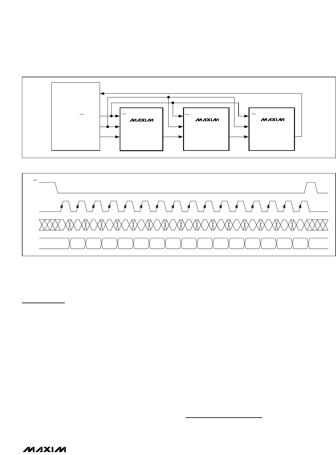
4-Wire-Interfaced, 2.5V to 5.5V, 20-Port and
28-Port I/O Expander
8 _______________________________________________________________________________________