8-Channel Source Drivers
2981 and
2982
4
Allegro MicroSystems, Inc.
115 Northeast Cutoff
Worcester, Massachusetts 01615-0036 U.S.A.
1.508.853.5000; www.allegromicro.com
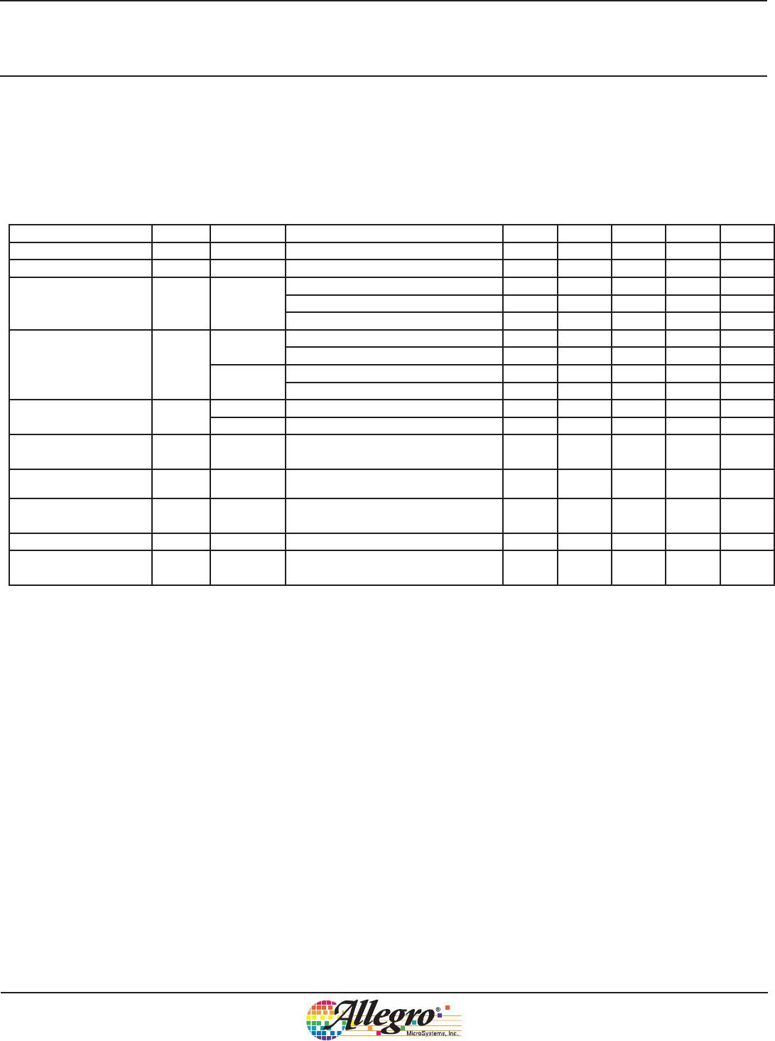
ELECTRICAL CHARACTERISTICS
1,2
at T
A
= +25°C (unless otherwise specifi ed).
1
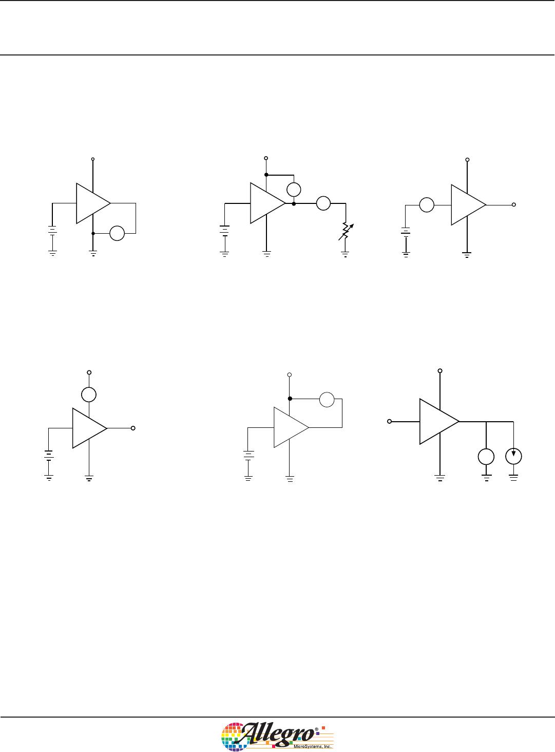
Negative current is defi ned as coming out of (sourcing) the specifi ed device terminal.
2
All unused inputs must be connected to ground. Pull-down resistors (approximately 10 kΩ) are recommended for inputs that are al-
lowed to fl oat while power is being applied to V
S
.
3
All inputs simultaneously.
4
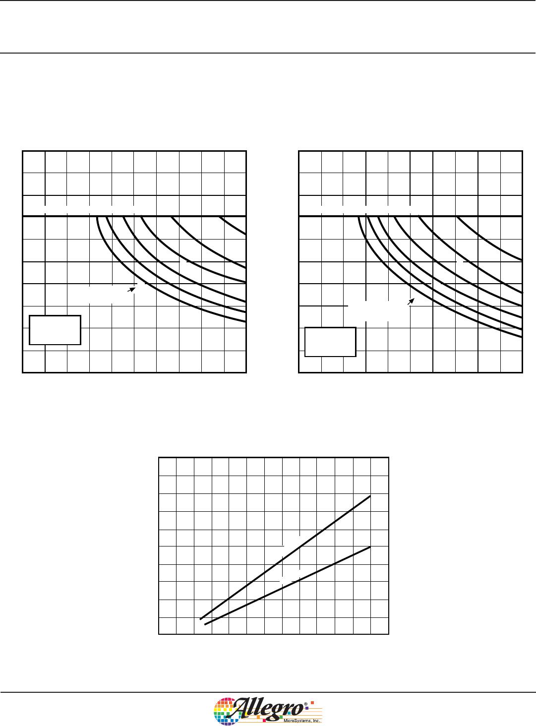
Turn-off delay is infl uenced by load conditions. Systems applications well below the specifi ed output loading may require timing con-
siderations for some designs, i.e., multiplexed displays or when used in combination with sink drivers in a totem pole confi guration.
Characteristic Symbol Variant Test Conditions Test Fig. Min. Typ. Max. Units
Output Leakage Current
3
I
CEX
All V
IN
= 0.4 V, V
S
= 50 V 1 — — 20 μA
Output Sustaining Voltage V
CE(SUS)
All I
OUT
= -45 mA — 35 — — V
Collector-Emitter
Saturation Voltage
V
CE(SAT)
All
V
IN
= 2.4 V, I
OUT
= -100 mA 2 — 1.6 1.8 V
V
IN
= 2.4 V, I
OUT
= -225 mA 2 — 1.7 1.9 V
V
IN
= 2.4 V, I
OUT
= -350 mA 2 — 1.8 2.0 V
Input Current I
IN(ON)
2981
V
IN
= 2.4 V 3 — 140 200 μA
V
IN
= 3.85 V 3 — 310 450 μA
2982
V
IN
= 2.4 V 3 — 140 200 μA
V
IN
= 12 V 3 — 1.25 1.93 mA
Output Source Current
(Outputs Open)
l
OUT
2981 V
IN
= 2.4 V, V
CE
= 2.0 V 2 -350 — — mA
2982 V
IN
= 2.4 V, V
CE
= 2.0 V 2 -350 — — mA
Supply Current Leakage
Current
I
S
All V
IN
= 2.4 V*, V
S
= 50 V 4 — — 10 mA
Clamp Diode Current I
R
All V
R
= 50 V, V
IN
= 0.4 V* 5 — — 50 μA
Clamp Diode Forward
Voltage
V
F
All I
F
= 350 mA 6 — 1.5 2.0 V
Turn-On Delay t
ON
All 0.5 E
IN
to 0.5 E
OUT
, R
L
= 100Ω, V
S
= 35 V — — 0.3 2.0 μs
Turn-Off Delay
4
t
OFF
All
0.5 E
IN
to 0.5 E
OUT
, R
L
= 100Ω, V
S
= 35 V,
See Note
— — 2.0 10 μs