ESD9B5.0ST5G

© Semiconductor Components Industries, LLC, 2011
December, 2011 Rev. 2
1 Publication Order Number:
ESD9B/D
ESD9B, SZESD9B
Transient Voltage
Suppressors
MicroPackaged Diodes for ESD Protection
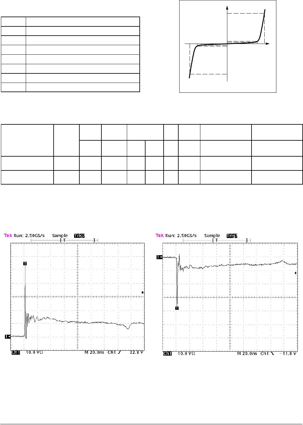
The ESD9B Series is designed to protect voltage sensitive
components from ESD. Excellent clamping capability, low leakage,
and fast response time provide best in class protection on designs that
are exposed to ESD. Because of its small size, it is suited for use in
cellular phones, MP3 players, digital cameras and many other portable
applications where board space comes at a premium.
Specification Features
Low Capacitance 15 pF
Low Clamping Voltage
Small Body Outline Dimensions: 0.039x 0.024 (1.0mm x 0.60mm)
Low Body Height: 0.016 (0.4 mm)
Standoff Voltage: 3.3 V, 5 V
Low Leakage
Response Time is < 1 ns
IEC6100042 Level 4 ESD Protection
AECQ101 Qualified and PPAP Capable
SZ Prefix for Automotive and Other Applications Requiring Unique
Site and Control Change Requirements
This is a PbFree Device
Mechanical Characteristics
CASE:
Void-free, transfer-molded, thermosetting plastic
Epoxy Meets UL 94 V0
LEAD FINISH: 100% Matte Sn (Tin)
MOUNTING POSITION: Any
QUALIFIED MAX REFLOW TEMPERATURE: 260°C
Device Meets MSL 1 Requirements
MAXIMUM RATINGS
Rating Symbol Value Unit
IEC 6100042 (ESD) Contact
Air
±18
±18
kV
IEC 6100044 (EFT) 40 A
Total Power Dissipation on FR5 Board
(Note 1) @ T
A
= 25°C
Thermal Resistance, JunctiontoAmbient
°P
D
°
R
q
JA
300
400
mW
°C/W
Junction and Storage Temperature Range T
J
, T
stg
55 to +150 °C
Lead Solder Temperature Maximum
(10 Second Duration)
T
L
260 °C
Stresses exceeding Maximum Ratings may damage the device. Maximum
Ratings are stress ratings only. Functional operation above the Recommended
Operating Conditions is not implied. Extended exposure to stresses above the
Recommended Operating Conditions may affect device reliability.
1. FR5 = 1.0 x 0.75 x 0.62 in.
Device Package Shipping
ORDERING INFORMATION
http://onsemi.com
For information on tape and reel specifications,
including part orientation and tape sizes, please
refer to our Tape and Reel Packaging Specifications
Brochure, BRD8011/D.
http://onsemi.com
ESD9B3.3ST5G SOD923
(PbFree)
8000/Tape & Reel
SOD923
CASE 514AB
MARKING DIAGRAM
X = Specific Device Code
M Date Code
X M
ESD9B5.0ST5G SOD923
(PbFree)
8000/Tape & Reel
SZESD9B5.0ST5G SOD923
(PbFree)
8000/Tape & Reel
BiDirectional TVS
I
PP
I
PP
V
I
I
R
I
T
I
T
I
R
V
RWM
V
C
V
BR
V
RWM
V
C
V
BR
ESD9B, SZESD9B
http://onsemi.com
2
ELECTRICAL CHARACTERISTICS
(T
A
= 25°C unless otherwise noted)
Symbol Parameter
I
PP
Maximum Reverse Peak Pulse Current
V
C
Clamping Voltage @ I
PP
V
RWM
Working Peak Reverse Voltage
I
R
Maximum Reverse Leakage Current @ V
RWM
V
BR
Breakdown Voltage @ I
T
I
T
Test Current
C Capacitance @ V
R
= 0 V and f = 1.0 MHz
ELECTRICAL CHARACTERISTICS (T
A
= 25°C unless otherwise noted)
Device
Device
Marking
V
RWM
(V)
I
R
(mA)
@ V
RWM
V
BR
(V) @ I
T
(Note 2)
I
T
C (pF) V
C
V
C
(V) @ I
PP
= 1 A
Max Max Min Max mA Typ
Per IEC6100042
(Note 3)
Max Per 8 x 20 ms
(Note 4)
ESD9B3.3ST5G 2* 3.3 1.0 5.0 7.0 1.0 15 Figures 1 and 2
See Below
10.5
ESD9B5.0ST5G,
SZESD9B5.0ST5G
E 5.0 1.0 5.8 7.8 1.0 15 Figures 1 and 2
See Below
12.5
* Rotated 270°.
2. V
BR
is measured with a pulse test current I
T
at an ambient temperature of 25°C.
3. For test procedure see Figures 3 and 4 and Application Note AND8307/D.
4. Surge current waveforms per Figure 5.
Figure 1. ESD Clamping Voltage Screenshot
Positive 8 kV Contact per IEC6100042
Figure 2. ESD Clamping Voltage Screenshot
Negative 8 kV Contact per IEC6100042
ESD9B, SZESD9B
http://onsemi.com
3
IEC 6100042 Spec.
Level
Test
Voltage
(kV)
First Peak
Current
(A)
Current at
30 ns (A)
Current at
60 ns (A)
1 2 7.5 4 2
2 4 15 8 4
3 6 22.5 12 6
4 8 30 16 8
I
peak
90%
10%
IEC6100042 Waveform
100%
I @ 30 ns
I @ 60 ns
t
P
= 0.7 ns to 1 ns
Figure 3. IEC6100042 Spec
Figure 4. Diagram of ESD Test Setup
50 W
50 W
Cable
TVS
Oscilloscope
ESD Gun
The following is taken from Application Note
AND8308/D Interpretation of Datasheet Parameters
for ESD Devices.
ESD Voltage Clamping
For sensitive circuit elements it is important to limit the
voltage that an IC will be exposed to during an ESD event
to as low a voltage as possible. The ESD clamping voltage
is the voltage drop across the ESD protection diode during
an ESD event per the IEC6100042 waveform. Since the
IEC6100042 was written as a pass/fail spec for larger
systems such as cell phones or laptop computers it is not
clearly defined in the spec how to specify a clamping voltage
at the device level. ON Semiconductor has developed a way
to examine the entire voltage waveform across the ESD
protection diode over the time domain of an ESD pulse in the
form of an oscilloscope screenshot, which can be found on
the datasheets for all ESD protection diodes. For more
information on how ON Semiconductor creates these
screenshots and how to interpret them please refer to
AND8307/D.
Figure 5. 8 X 20 ms Pulse Waveform
100
90
80
70
60
50
40
30
20
10
0
020406080
t, TIME (ms)
% OF PEAK PULSE CURRENT
t
P
t
r
PULSE WIDTH (t
P
) IS DEFINED
AS THAT POINT WHERE THE
PEAK CURRENT DECAY = 8 ms
PEAK VALUE I
RSM
@ 8 ms
HALF VALUE I
RSM
/2 @ 20 ms

ESD9B5.0ST5G

Mfr. #:
Manufacturer:
ON Semiconductor
Description:
TVS Diodes / ESD Suppressors BiDIRECTIONAL ESD PROTECTION
Lifecycle:
New from this manufacturer.
Delivery:
DHL FedEx Ups TNT EMS
Payment:
T/T Paypal Visa MoneyGram Western Union

Products related to this Datasheet