1
LT1112/LT1114
111214fb
Dual/Quad Low Power
Precision, Picoamp Input Op Amps
The LT
®
1112 dual and LT1114 quad op amps achieve a
new standard in combining low cost and outstanding
precision specifications.
The performance of the selected prime grades matches or
exceeds competitive devices. In the design of the LT1112/
LT1114 however, particular emphasis has been placed on
optimizing performance in the low cost plastic and SO
packages. For example, the 75µV maximum offset voltage
in these low cost packages is the lowest on any dual or
quad non-chopper op amp.
The LT1112/LT1114 also provide a full set of matching
specifications, facilitating their use in such matching
dependent applications as two and three op amp instru-
mentation amplifiers.
Another set of specifications is furnished at ±1V supplies.
This, combined with the low 320µA supply current per
amplifier, allows the LT1112/LT1114 to be powered by
two nearly discharged AA cells.
Offset Voltage – Prime Grade: 60µV Max
Offset Voltage – Low Cost Grade
(Including Surface Mount Dual/Quad): 75µV Max
Offset Voltage Drift: 0.5µV/°C Max
Input Bias Current: 250pA Max
0.1Hz to 10Hz Noise: 0.3µV
P-P
, 2.2pA
P-P
Supply Current per Amplifier: 400µA Max
CMRR: 120dB Min
Voltage Gain: 1 Million Min
Guaranteed Specs with ±1.0V Supplies
Guaranteed Matching Specifications
SO-8 Package – Standard Pinout
LT1114 in Narrow Surface Mount Package
Picoampere/Microvolt Instrumentation
Two and Three Op Amp Instrumentation Amplifers
Thermocouple and Bridge Amplifiers
Low Frequency Active Filters
Photo Current Amplifiers
Battery-Powered Systems
Protected by U.S. Patents 4,575,685; 4,775,884 and 4,837,496
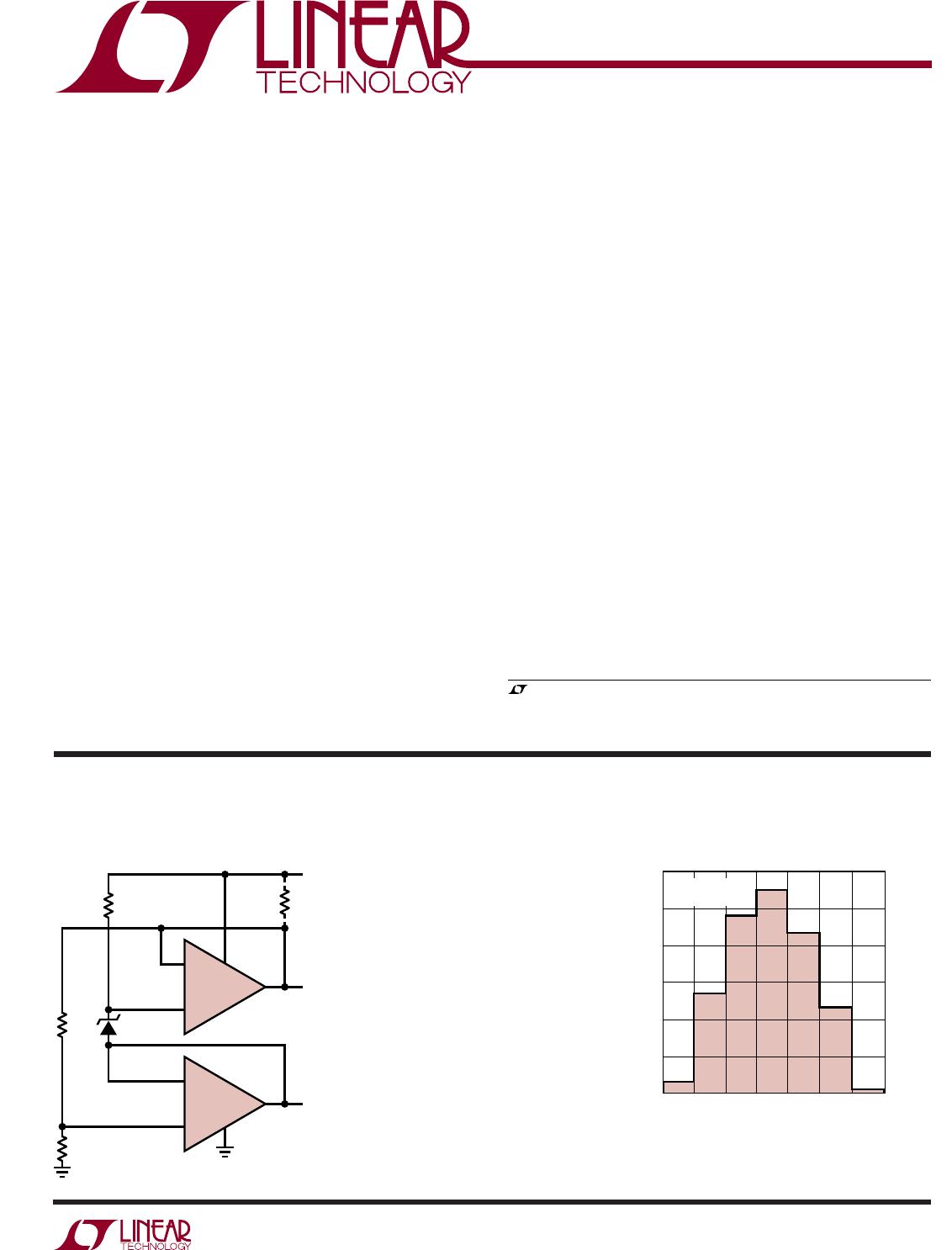
Distribution of Input Offset Voltage
(In All Packages)
INPUT OFFSET VOLTAGE (µV)
–70
PERCENT OF UNITS
20
25
30
–10 30
15
10
–50 –30
10 50 70
5
0
V
S
= ±15V
T
A
= 25°C
LT1112/14 • TA02
+
1/2 LT1112
+
1/2 LT1112
LT1004-1.2
75k
0.1%
46.4k
0.1%
2
3
6
5
4
7
8
1
0.765V
R
X
15k
3V
2.000V
LT1112/14 • TA01
TOTAL SUPPLY CURRENT = 700µA
2V REFERENCE: SOURCES 1.7mA, SINKS 5mA
OPTIONAL R
X
= 300 INCREASES SOURCE
CURRENT TO 5mA
0.765V REFERENCE: SOURCES 5mA,
SINKS 0.5mA
TEMPERATURE COEFFICIENT LIMITED
BY REFERENCE = 20ppm/°C
MINIMUM SUPPLY = 2.7V
Dual Output, Buffered Reference (On Single 3V Supply)
DESCRIPTIO
U
FEATURES
APPLICATIO S
U
TYPICAL APPLICATIO
U
, LT, LTC and LTM are registered trademarks of Linear Technology Corporation.
2
LT1112/LT1114
111214fb
ORDER PART
NUMBER
ORDER PART
NUMBER
S8 PART MARKING
T
JMAX
= 150°C, θ
JA
= 190°C/W
LT1112S8
LT1112IS8
LT1112MPS8
LT1112ACN8
LT1112CN8
LT1112IN8
1112
1112I
1112MP
ORDER PART
NUMBER
ORDER PART
NUMBER
LT1114S
LT1114IS
LT1114ACN
LT1114CN
LT1114IN
T
JMAX
= 150°C, θ
JA
= 110°C/W
J8 PACKAGE 8-LEAD CERDIP
T
JMAX
= 160°C, θ
JA
= 100°C/W
T
JMAX
= 150°C, θ
JA
= 150°C/W
TOP VIEW
OUT A
IN A
+IN A
V
V
+
OUT B
–IN B
+IN B
N8 PACKAGE
8-LEAD PDIP
1
2
3
4
8
7
6
5
A
B
1
2
3
4
5
6
7
TOP VIEW
N PACKAGE
14-LEAD PDIP
14
13
12
11
10
9
8
OUT A
–IN A
+IN A
V
+
+IN B
IN B
OUT B
OUT D
IN D
+IN D
V
+IN C
IN C
OUT C
A
D
B
C
1
2
3
4
8
7
6
5
TOP VIEW
V
+
OUT B
IN B
+IN B
OUT A
IN A
+IN A
V
S8 PACKAGE
8-LEAD PLASTIC SO
B
A
TOP VIEW
S PACKAGE
16-LEAD PLASTIC SO (NARROW)
1
2
3
4
5
6
7
8
16
15
14
13
12
11
10
9
OUT A
IN A
+IN A
V
+
+IN B
IN B
OUT B
NC
OUT D
IN D
+IN D
V
+IN C
IN C
OUT C
NC
A
D
B
C
(Note 1)
ABSOLUTE AXI U RATI GS
WWWU
LT1112AMJ8
LT1112MJ8
T
JMAX
= 150°C, θ
JA
= 130°C/W
OBSOLETE PACKAGE
Consider the N8 Package for Alternate Source
LT1114AMJ
LT1114MJ
J PACKAGE 14-LEAD CERDIP
T
JMAX
= 160°C, θ
JA
= 80°C/W (J)
OBSOLETE PACKAGE
Consider the N Package for Alternate Source
PACKAGE/ORDER I FOR ATIO
UU
W
Consult LTC Marketing for parts specified with wider operating temperature ranges.
Supply Voltage ..................................................... ±20V
Differential Input Current (Note 2) ..................... ±10mA
Input Voltage (Equal to Supply Voltage) ............... ±20V
Output Short-Circuit Duration ......................... Indefinite
Storage Temperature Range ................ 65°C to 150°C
Lead Temperature (Soldering, 10 sec)................ 300°C
Operating Temperature Range (Note 11)
LT1112AM/LT1112M
LT1114AM/LT1114M (OBSOLETE)... 55°C to 125°C
LT1112AC/LT1112C/LT1112S8
LT1114AC/LT1114C/LT1114S .......... 40°C to 85°C
LT1112I/LT1114I .............................. 40°C to 85°C
LT1112MPS8 ................................... –55°C to 125°C
Specified Temperature Range (Note 12)
LT1112AM/LT1112M
LT1114AM/LT1114M (OBSOLETE)... 55°C to 125°C
LT1112AC/LT1112C/LT1112S8
LT1114AC/LT1114C/LT1114S .......... 40°C to 85°C
LT1112I/LT1114I .............................. 40°C to 85°C
LT1112MPS8 ................................... –55°C to 125°C
3
LT1112/LT1114
111214fb
SYMBOL PARAMETER CONDITIONS (Note 3) MIN TYP MAX MIN TYP MAX UNITS
V
OS
Input Offset Voltage 20 60 25 75 µV
V
S
= ±1.0V 40 110 45 130 µV
V
OS
Long Term Input Offset 0.3 0.3 µV/Mo
Time Voltage Stability
I
OS
Input Offset Current 50 180 60 230 pA
LT1114S/LT1114IS 75 330 pA
I
B
Input Bias Current ±70 ±250 ±80 ±280 pA
LT1114S/LT1114IS ±100 ±450 pA
e
n
Input Noise Voltage 0.1Hz to 10Hz (Note 10) 0.3 0.9 0.3 0.9 µV
P-P
Input Noise Voltage Density f
O
= 10Hz (Note 10) 16 28 16 28 nV/Hz
f
O
= 1000Hz (Note 10) 14 18 14 18 nV/Hz
i
n
Input Noise Current 0.1Hz to 10Hz 2.2 2.2 pA
P-P
Input Noise Current Density f
O
= 10Hz 0.030 0.030 pA/Hz
f
O
= 1000Hz 0.008 0.008 pA/Hz
V
CM
Input Voltage Range ±13.5 ±14.3 ±13.5 ±14.3 V
CMRR Common Mode Rejection Ratio V
CM
= ±13.5V 120 136 115 136 dB
PSRR Power Supply Rejection Ratio V
S
= ±1.0V to ±20V 116 126 114 126 dB
Minimum Supply Voltage (Note 5) ±1.0 ± 1.0 V
R
IN
Input Resistance
Differential Mode (Note 4) 20 50 15 40 M
Common Mode 800 700 G
A
VOL
Large-Signal Voltage Gain V
O
= ±12V, R
L
= 10k 1000 5000 800 5000 V/mV
V
O
= ±10V, R
L
= 2k 800 1500 600 1300 V/mV
V
OUT
Output Voltage Swing R
L
= 10k ±13.0 ±14.0 ±13.0 ±14.0 V
R
L
= 2k ±11.0 ±12.4 ±11.0 ±12.4 V
SR Slew Rate 0.16 0.30 0.16 0.30 V/µs
GBW Gain-Bandwidth Product f
O
= 10kHz 450 750 450 750 kHz
I
S
Supply Current per Amplifier 350 400 350 450 µA
V
S
= ±1.0V 320 370 320 420 µA
Channel Separation f
O
= 10Hz 150 150 dB
V
OS
Offset Voltage Match (Note 6) 35 100 40 130 µV
I
B
+
Noninverting Bias Current Match 100 450 100 500 pA
(Notes 6, 7) LT1114S/LT1114IS 120 680 pA
CMRR Common Mode Rejection Match (Notes 6, 8) 117 136 113 136 dB
PSRR Power Supply Rejection Match (Notes 6, 8) 114 130 112 130 dB
V
S
= ±15V, V
CM
= 0V, T
A
= 25°C, unless otherwise noted.
LT1112AM/AC
LT1114AM/AC
LT1112M/C/I
LT1114M/C/I
ELECTRICAL CHARACTERISTICS

LT1112IS8#PBF

Mfr. #:
Manufacturer:
Analog Devices Inc.
Description:
Precision Amplifiers 2x L Pwr Prec, pA In Op Amps
Lifecycle:
New from this manufacturer.
Delivery:
DHL FedEx Ups TNT EMS
Payment:
T/T Paypal Visa MoneyGram Western Union