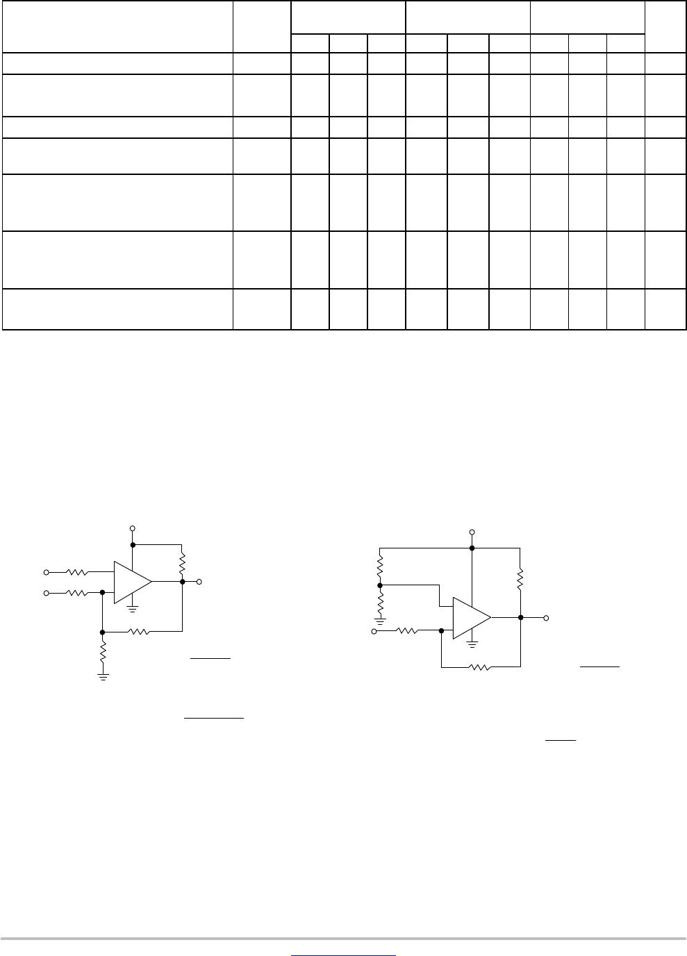
LM339, LM339E, LM239, LM2901, LM2901E, LM2901V, NCV2901, MC3302
www.onsemi.com
4
PERFORMANCE CHARACTERISTICS (V
CC
= +5.0 Vdc, T
A
= T
low
to T
high
[Note 7])
Characteristic Symbol
LM239/339/339E
LM2901/2901E/2901V
/NCV2901
MC3302
Unit
Min Typ Max Min Typ Max Min Typ Max
Input Offset Voltage (Note 8) V
IO
− − ±9.0 − − ±15 − − ±40 mVdc
Input Bias Current (Notes 8, 9) I
IB
− − 400 − − 500 − − 1000 nA
(Output in Analog Range)
Input Offset Current (Note 8) I
IO
− − ±150 − − ±200 − − ±300 nA
Input Common Mode Voltage Range V
ICMR
0 − V
CC
−2.0
0 − V
CC
−2.0
0 − V
CC
−2.0
V
Saturation Voltage V
sat
− − 700 − − 700 − − 700 mV
V
I
(−) ≥ +1.0 Vdc, V
I
(+) = 0,
I
sink
≤ 4.0 mA
Output Leakage Current I
OL
− − 1.0 − − 1.0 − − 1.0
mA
V
I
(+) ≥ +1.0 Vdc, V
I
(−) = 0,
V
O
= 30 Vdc
Differential Input Voltage V
ID
− − V
CC
− − V
CC
− − V
CC
Vdc
All V
I
≥ 0 Vdc
7. (LM239) T
low
= −25°C, T
high
= +85°
(LM339, LM339E) T
low
= 0°C, T
high
= +70°C
(MC3302) T
low
= −40°C, T
high
= +85°C
(LM2901, LM2901E) T
low
= −40°C, T
high
= +105°
(LM2901V & NCV2901) T
low
= −40°C, T
high
= +125°C
NCV2901 is qualified for automotive use.
8. At the output switch point, V
O
] 1.4 Vdc, R
S
≤ 100 W 5.0 Vdc ≤ V
CC
≤ 30 Vdc, with the inputs over the full common mode range
(0 Vdc to V
CC
−1.5 Vdc).
9. The bias current flows out of the inputs due to the PNP input stage. This current is virtually constant, independent of the output state.
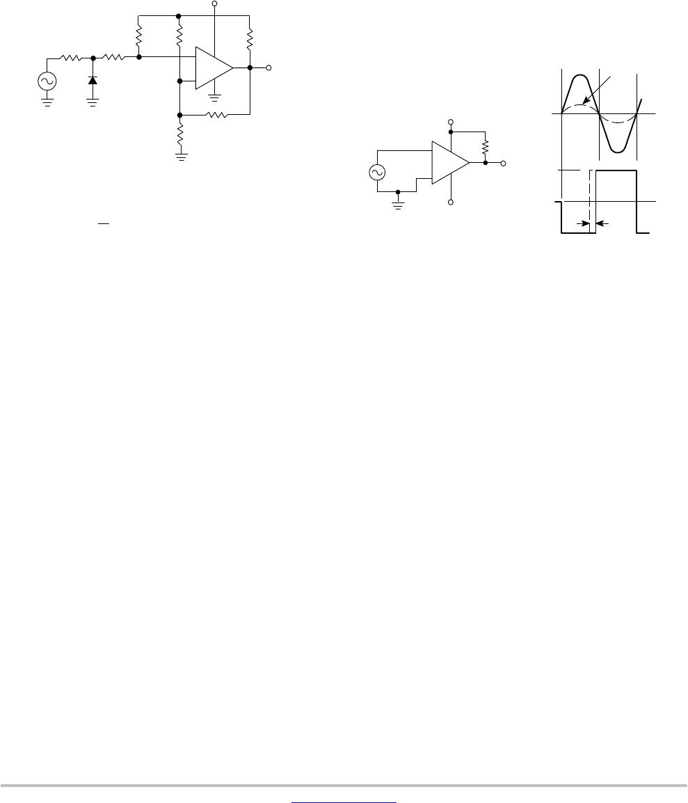
Figure 2. Inverting Comparator
with Hysteresis
Figure 3. Noninverting Comparator
with Hysteresis
V
ref
=
V
CC
R1
R
ref
+ R1
R2 [ R1 / / R
ref
Amount of Hysteresis V
H
V
H
=
R2
R2 + R3
[(V
O(max)
- V
O(min)
]
V
ref
[
V
CC
R1
R
ref
+ R1
R3 ] R1 / / R
ref
/ / R2
V
H
=
R1 / / R
ref
R1/ / R
ref
+ R2
[V
O(max)
- V
O(min)
]
R2 ơ Rref / / R1
+ V
CC
Vi
n
V
ref
+ V
CC
+ V
CC
V
in
V
ref
R
ref
R
ref
-
+
-
+
V
O
V
O
10k
R1
R2
R3
10 k
1.0 M
R3
R2
1.0 M
10 k
R1
10 k
10 k