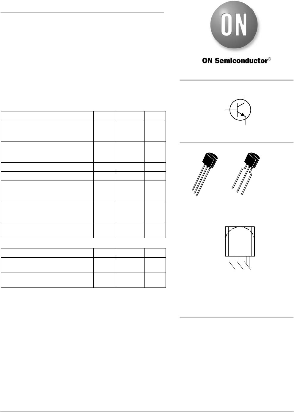
MPSA42G

© Semiconductor Components Industries, LLC, 2013
February, 2013 Rev. 8
1 Publication Order Number:
MPSA42/D
MPSA42, MPSA43
High Voltage Transistors
NPN Silicon
Features
These are PbFree Devices*
MAXIMUM RATINGS
Rating Symbol Value Unit
CollectorEmitter Voltage
MPSA43
MPSA42
V
CEO
200
300
Vdc
CollectorBase Voltage
MPSA43
MPSA42
V
CBO
200
300
Vdc
EmitterBase Voltage V
EBO
6.0 Vdc
Collector Current Continuous I
C
500 mAdc
Total Device Dissipation
@ T
A
= 25°C
Derate above 25°C
P
D
625
5.0
mW
mW/°C
Total Device Dissipation
@ T
C
= 25°C
Derate above 25°C
P
D
1.5
12
W
mW/°C
Operating and Storage Junction
Temperature Range
T
J
, T
stg
55 to
+150
°C
THERMAL CHARACTERISTICS
Characteristic Symbol Max Unit
Thermal Resistance,
JunctiontoAmbient
R
q
JA
200 °C/W
Thermal Resistance,
JunctiontoCase
R
q
JC
83.3 °C/W
Stresses exceeding Maximum Ratings may damage the device. Maximum
Ratings are stress ratings only. Functional operation above the Recommended
Operating Conditions is not implied. Extended exposure to stresses above the
Recommended Operating Conditions may affect device reliability.
*For additional information on our PbFree strategy and soldering details, please
download the ON Semiconductor Soldering and Mounting Techniques
Reference Manual, SOLDERRM/D.
http://onsemi.com
x = 2 or 3
A = Assembly Location
Y = Year
WW = Work Week
G = PbFree Package
(Note: Microdot may be in either location)
See detailed ordering and shipping information in the package
dimensions section on page 3 of this data sheet.
ORDERING INFORMATION
COLLECTOR
3
2
BASE
1
EMITTER
MARKING DIAGRAM
MPS
A4x
AYWWG
G
TO92
(TO226AA)
CASE 2911
1
2
3
1
2
BENT LEADSTRAIGHT LEAD
3
MPSA42, MPSA43
http://onsemi.com
2
ELECTRICAL CHARACTERISTICS (T
A
= 25°C unless otherwise noted)
Characteristic
Symbol Min Max Unit
OFF CHARACTERISTICS
CollectorEmitter Breakdown Voltage (Note 1)
(I
C
= 1.0 mAdc, I
B
= 0) MPSA42
MPSA43
V
(BR)CEO
300
200
Vdc
CollectorBase Breakdown Voltage
(I
C
= 100 mAdc, I
E
= 0) MPSA42
MPSA43
V
(BR)CBO
300
200
Vdc
EmitterBase Breakdown Voltage
(I
E
= 100 mAdc, I
C
= 0)
V
(BR)EBO
6.0 Vdc
Collector Cutoff Current
(V
CB
= 200 Vdc, I
E
= 0) MPSA42
(V
CB
= 160 Vdc, I
E
= 0) MPSA43
I
CBO
0.1
0.1
mAdc
Emitter Cutoff Current
(V
EB
= 6.0 Vdc, I
C
= 0) MPSA42
(V
EB
= 4.0 Vdc, I
C
= 0) MPSA43
I
EBO
0.1
0.1
mAdc
ON CHARACTERISTICS (Note 1)
DC Current Gain
(I
C
= 1.0 mAdc, V
CE
= 10 Vdc)
(I
C
= 10 mAdc, V
CE
= 10 Vdc)
(I
C
= 30 mAdc, V
CE
= 10 Vdc)
h
FE
25
40
40
CollectorEmitter Saturation Voltage
(I
C
= 20 mAdc, I
B
= 2.0 mAdc) MPSA42
MPSA43
V
CE(sat)
0.5
0.4
Vdc
BaseEmitter Saturation Voltage
(I
C
= 20 mAdc, I
B
= 2.0 mAdc)
V
BE(sat)
0.9 Vdc
SMALLSIGNAL CHARACTERISTICS
CurrentGain Bandwidth Product
(I
C
= 10 mAdc, V
CE
= 20 Vdc, f = 100 MHz)
f
T
50 MHz
CollectorBase Capacitance
(V
CB
= 20 Vdc, I
E
= 0, f = 1.0 MHz) MPSA42
MPSA43
C
cb
3.0
4.0
pF
1. Pulse Test: Pulse Width v 300 ms, Duty Cycle v 2%.
MPSA42, MPSA43
http://onsemi.com
3
ORDERING INFORMATION
Device Package Shipping
MPSA42G TO92
(PbFree)
5000 Units / Box
MPSA42RL1G TO92
(PbFree)
2000 / Tape & Reel
MPSA42RLRAG TO92
(PbFree)
2000 / Tape & Reel
MPSA42RLRMG TO92
(PbFree)
2000 / Ammo Pack
MPSA42RLRPG TO92
(PbFree)
2000 / Ammo Pack
MPSA42ZL1G TO92
(PbFree)
2000 / Ammo Pack
For information on tape and reel specifications, including part orientation and tape sizes, please refer to our Tape and Reel Packaging
Specifications Brochure, BRD8011/D.

MPSA42G

Mfr. #:
Manufacturer:
ON Semiconductor
Description:
Bipolar Transistors - BJT 500mA 300V NPN
Lifecycle:
New from this manufacturer.
Delivery:
DHL FedEx Ups TNT EMS
Payment:
T/T Paypal Visa MoneyGram Western Union