7
Recommended Operating Conditions
Parameter Symbol Min. Max. Units
Power Supply Voltage V
CC
4.5 20 V
Enable Voltage High V
EH
2.0 20 V
Enable Voltage Low V
EL
00.8 V
Forward Input Current I
F(ON)
1.6* 5 mA
Forward Input Current I
F(OFF)
–0.1 mA
Operating Temperature T
A
085
[1]
°C
Fan Out N 4 TTL Loads
*The initial switching threshold is 1.6 mA or less. It is recommended that 2.2 mA be used to permit
at least a 20% CTR degradation guardband.
Absolute Maximum Ratings
(No Derating Required up to 70°C)
Parameter Symbol Min. Max. Units Note
Storage Temperature T
S
-55 125 °C
Operating Temperature T
A
-40 85 °C1
Average Forward Input Current I
F(AVG)
10 mA
Peak Transient Input Current I
F(TRAN)
1.0 A
(1 µs Pulse Width, 300 pps)
Reverse Input Voltage V
R
5V
Average Output Current I
O
25 mA
Supply Voltage V
CC
020V
Three State Enable Voltage V
E
-0.5 20 V
Output Voltage V
O
-0.5 20 V
Total Package Power Dissipation P
T
210 mW 1
Lead Solder Temperature 260°C for 10 sec., 1.6 mm below seating plane
Solder Reflow Temperature Profile See Package Outline Drawings section
8
Electrical Specifications
For 0°C T
A
[1]
85°C, 4.5 V V
CC
20 V, 1.6 mA I
F(ON)
5 mA, 2.0 V V
EH
20 V, 0.0 V V
EL
0.8 V, 0 mA I
F(OFF)
0.1 mA.
All Typicals at T
A
= 25°C, V
CC
= 5 V, I
F(ON)
= 3 mA unless otherwise specified. See Note 7.
Parameter Sym. Min. Typ. Max. Units Test Conditions Fig. Note
Logic Low V
OL
0.5 V I
OL
= 6.4 mA (4 TTL Loads) 1
Output Voltage
Logic High V
OH
2.4 * V I
OH
= -2.6 mA *V
OH
= V
CC
- 2.1 V 2
Output Voltage
Output Leakage I
OHH
100 µAV
O
= 5.5 V I
F
= 5 mA
Current (V
OUT
> V
CC
)V
CC
= 4.5 V
Logic High Enable V
EH
2.0 V
Voltage
Logic Low Enable V
EL
0.8 V
Voltage
Logic High Enable I
EH
20 µAV
EN
= 2.7 V
Current
Logic Low Enable I
EL
-0.32 mA V
EN
= 0.4 V
Current
Logic Low Supply I
CCL
I
F
= 0 mA
Current I
O
= Open
V
E
= Don’t Care
Logic High Supply I
CCH
I
F
= 5 mA
Current I
O
= Open
V
E
= Don’t Care
High Impedance I
OZL
-20 µAV
O
= 0.4 V V
EN
= 2 V,
I
F
= 5 mA
I
OZH
20 µAV
O
= 2.4 V V
EN
= 2 V,
100 µAV
O
= 5.5 V
500 µAV
O
= 20 V
Logic Low Short I
OSL
2
Circuit Output
Current
Logic High Short I
OSH
I
F
= 5 mA, 2
Circuit Output V
O
= GND
Current
Input Current I
HYS
0.12 mA V
CC
= 5 V 3
Hysteresis
Input Forward V
F
1.5 1.7 V T
A
= 25°CI
F
= 5 mA 4
1.75
Input Reverse BV
R
5VI
R
= 10 µA
Breakdown Voltage
Input Diode V
F
-1.7 mV/°CI
F
= 5 mA
Temperature T
A
Coefficient
Input Capacitance C
IN
60 pF f = 1 MHz, V
F
= 0 V, Pins 2 and 3
mA V
O
= V
CC
= 5.5 V I
F
= 0 mA
25
500 µA V
O
= 20 V
100 µAV
EN
= 5.5 V
250 µAV
EN
= 20 V0.004
6.0 mA V
CC
= 5.5 V4.5
5.25
6.0 mA V
CC
= 20 V
4.5 mA V
CC
= 5.5 V
2.7
3.1
State Output Current
mA V
O
= V
CC
= 20 V
40
mA V
CC
= 5.5 V
-10
mA V
CC
= 20 V
-25
Voltage
7.5 mA V
CC
= 20 V
I
F
= 5 mA
9
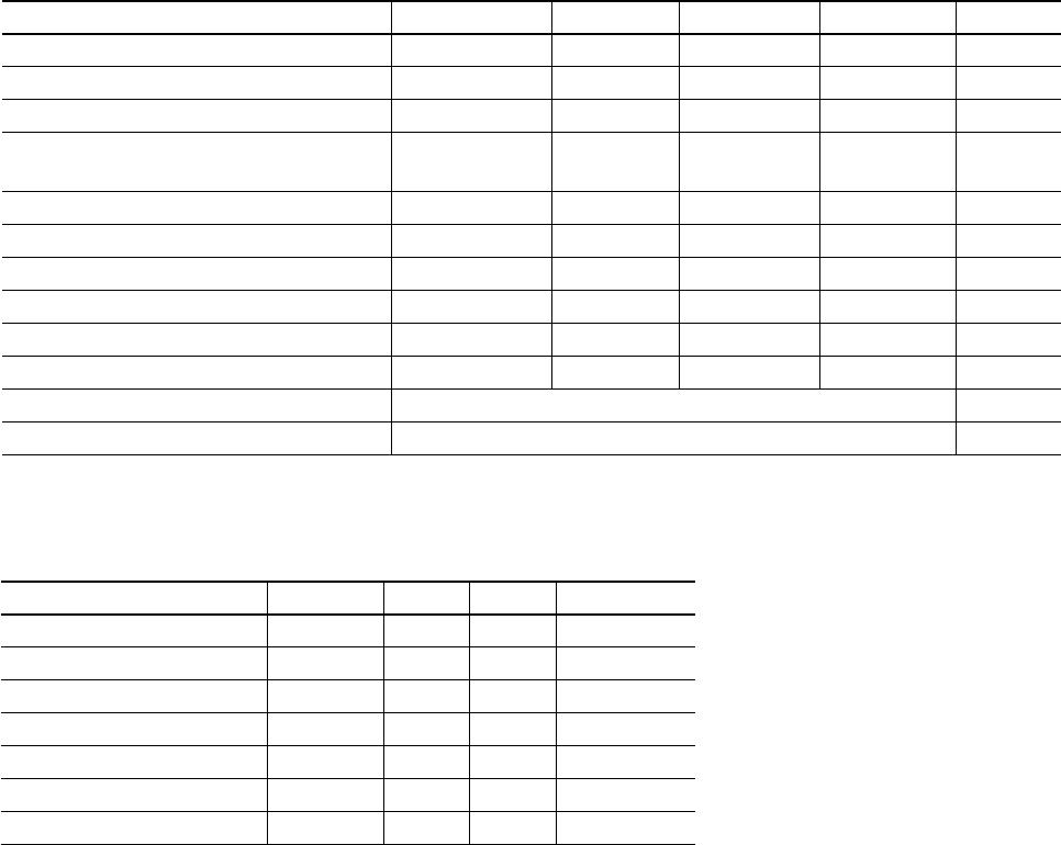
Switching Specifications (AC)
For 0°C T
A
[1]
85°C, 4.5 V V
CC
20 V, 1.6 mA I
F(ON)
5 mA, 0.0 mA I
F(OFF)
0.1 mA.
All Typicals at T
A
= 25°C, V
CC
= 5 V, I
F(ON)
= 3 mA unless otherwise specified.
Parameter Sym. Min. Typ. Max. Units Test Conditions Fig. Note
Propagation Delay Time to t
PHL
210 ns Without Peaking Capacitor 5, 6 4, 5
160 300 With Peaking Capacitor
Propagation Delay Time to t
PLH
170 ns Without Peaking Capacitor 5, 6 4, 5
115 300 With Peaking Capacitor
Output Enable Time to t
PZH
25 ns 7, 9
Logic High
Output Enable Time to t
PZL
28 ns 7, 8
Logic Low
Output Disable Time from t
PHZ
105 ns 7, 9
Logic High
Output Disable Time from t
PLZ
60 ns 7, 8
Logic Low
Output Rise Time (10-90%) t
r
55 ns 5, 10
Output Fall Time (90-10%) t
f
15 ns 5, 10
Logic Low Output Level
Logic High Output Level
Package Characteristics
Parameter Sym. Min. Typ. Max. Units Test Conditions Fig. Note
Input-Output Momentary V
ISO
3750 V rms RH 50%, t = 1 min., 3, 8
Withstand Voltage* T
A
= 25°C
Input-Output Resistance R
I-O
10
12
V
I-O
= 500 VDC 3
Input-Output Capacitance C
I-O
0.6 pF f = 1 MHz, V
I-O
= 0 VDC 3
*The Input-Output Momentary Withstand Voltage is a dielectric voltage rating that should not be interpreted as an input-output continuous voltage rating. For
the continuous voltage rating refer to the IEC/EN/DIN EN 60747-5-2 Insulation Characteristics Table (if applicable), your equipment level safety specification
or Avago Application Note 1074 entitled “Optocoupler Input-Output Endurance Voltage,” publication number 5963-2203E.
Parameter Sym. Device Min. Units Test Conditions Fig. Note
Logic High |CM
H
|I
F
= 1.6 mA 11 6
Common Mode V
CC
= 5 V
Transient T
A
= 25°C
Immunity
Logic Low |CM
L
|V
F
= 0 V 11 6
Common Mode V
CC
= 5 V
Transient T
A
= 25°C
Immunity
HCPL-2200 1,000 V/µs |V
CM
| = 50 V
HCPL-2219 2,500 V/µs |V
CM
| = 400 V
HCPL-2200 1,000 V/µs |V
CM
| = 50 V
HCPL-2219 2,500 V/µs |V
CM
| = 400 V

HCPL-2200-500E

Mfr. #:
Manufacturer:
Broadcom / Avago
Description:
High Speed Optocouplers 5MBd 1Ch 1.6mA
Lifecycle:
New from this manufacturer.
Delivery:
DHL FedEx Ups TNT EMS
Payment:
T/T Paypal Visa MoneyGram Western Union