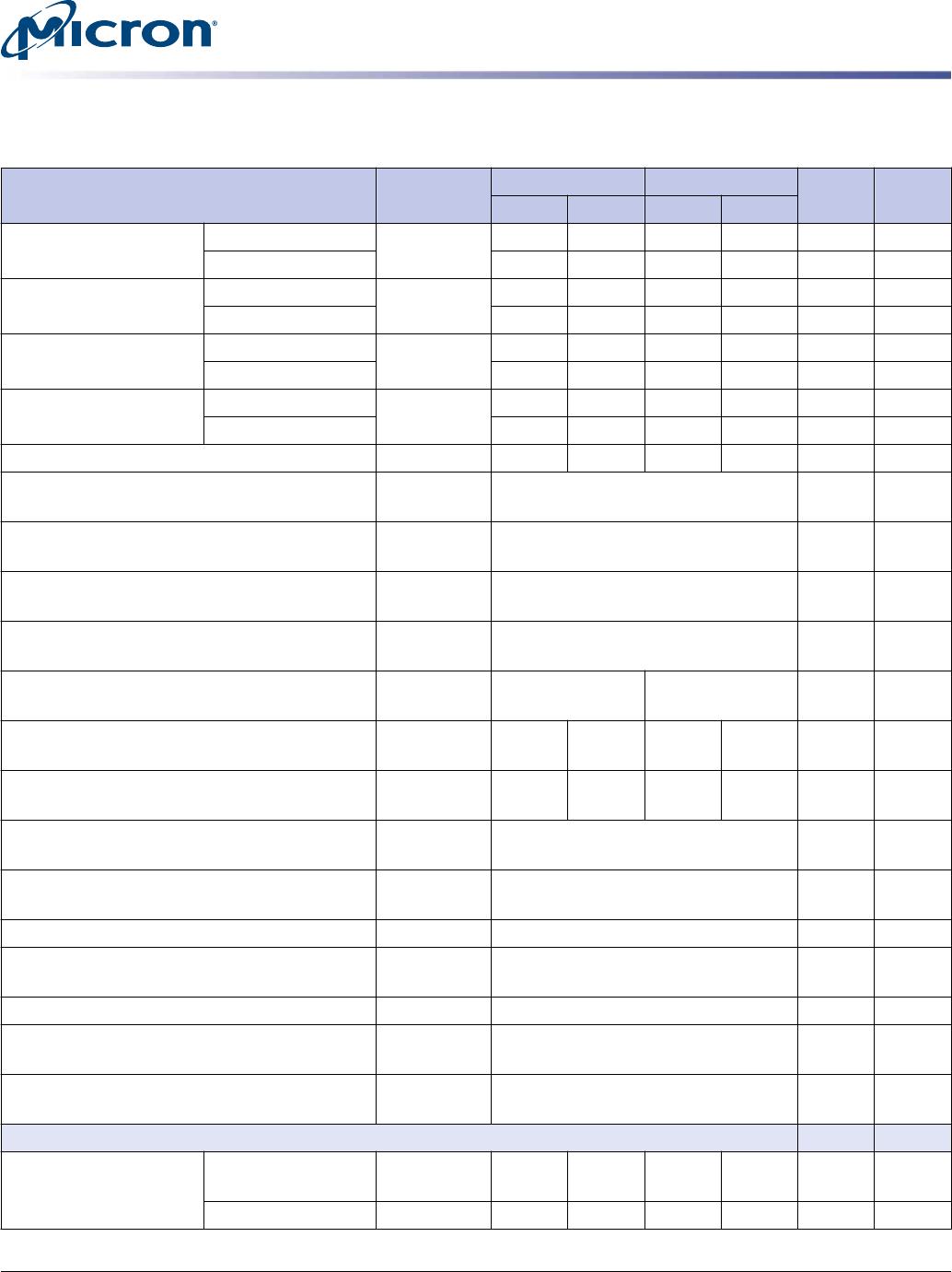
Table 11: Electrical Characteristics and AC Operating Conditions for Speed Extensions (Continued)
Notes 1–8 apply to the entire table
Parameter Symbol
gDDR3-2000 gDDR3-2200
Unit NotesMin Max Min Max
ACTIVATE command to power-down entry
t
ACTPDEN MIN = 2 MIN = 1 CK
PRECHARGE/PRECHARGE ALL command to
power-down entry
t
PRPDEN MIN = 2 MIN = 1 CK
REFRESH command to power-down entry
t
REFPDEN MIN = 2 MIN = 1 CK 37
MRS command to power-down entry
t
MRSPDEN MIN =
t
MOD (MIN) CK
READ/READ with auto precharge command to
power-down entry
t
RDPDEN MIN = RL + 4 + 1 CK
WRITE command to
power-down entry
BL8 (OTF, MRS)
BC4OTF
t
WRPDEN MIN = WL + 4 +
t
WR/
t
CK (AVG) CK
BC4MRS
t
WRPDEN MIN = WL + 2 +
t
WR/
t
CK (AVG) CK
WRITE with auto pre-
charge command to
power-down entry
BL8 (OTF, MRS)
BC4OTF
t
WRAPDEN MIN = WL + 4 + WR + 1 CK
BC4MRS
t
WRAPDEN MIN = WL + 2 + WR + 1 CK
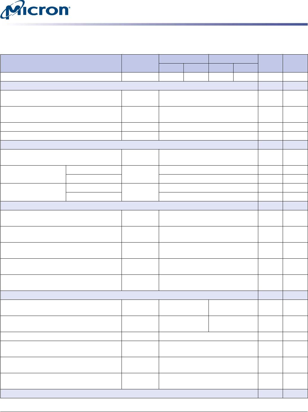
Power-Down Exit Timing
DLL on, any valid command, or DLL off to com-
mands not requiring locked DLL
t
XP MIN = greater of 3CK or 6ns; MAX =
N/A
CK
Precharge power-down with DLL off to com-
mands requiring a locked DLL
t
XPDLL MIN = greater of 10CK or 24ns; MAX =
N/A
CK 28
ODT Timing
R
TT
synchronous turn-on delay ODTL on CWL + AL - 2CK CK 38
R
TT
synchronous turn-off delay ODTL off CWL + AL - 2CK CK 40
R
TT
turn-on from ODTL on reference
t
AON –195 195 –195 195 ps 23, 38
R
TT
turn-off from ODTL off reference
t
AOF 0.3 0.7 0.3 0.7 CK 39, 40
Asynchronous R
TT
turn-on delay
(power-down with DLL off)
t
AONPD MIN = 2; MAX = 8.5 ns 38
Asynchronous R
TT
turn-off delay
(power-down with DLL off)
t
AOFPD MIN = 2; MAX = 8.5 ns 40
ODT HIGH time with WRITE command and BL8 ODTH8 MIN = 6; MAX = N/A CK
ODT HIGH time without WRITE command or
with WRITE command and BC4
ODTH4 MIN = 4; MAX = N/A CK
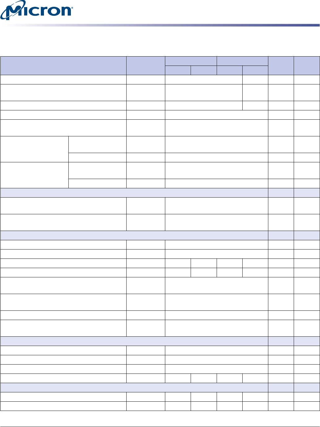
Dynamic ODT Timing
R
TT,nom
-to-R
TT(WR)
change skew ODTLcnw WL - 2CK CK
R
TT(WR)
-to-R
TT,nom
change skew - BC4 ODTLcnw4 4CK + ODTLoff CK
R
TT(WR)
-to-R
TT,nom
change skew - BL8 ODTLcnw8 6CK + ODTLoff CK
R
TT
dynamic change skew
t
ADC 0.3 0.7 0.3 0.7 CK 39
Write Leveling Timing
First DQS, DQS# rising edge
t
WLMRD 40 – 40 – CK
DQS, DQS# delay
t
WLDQSEN 25 – 25 – CK
4Gb: x16 gDDR3 SDRAM Graphics Addendum
Electrical Characteristics and AC Operating Conditions
CCMTD-1005363231-10344
ddr3_4gb_graphics_addendum 091.pdf - Rev. A 05/16 EN
15
Micron Technology, Inc. reserves the right to change products or specifications without notice.
© 2012 Micron Technology, Inc. All rights reserved.