74FCT20807QGI

4
INDUSTRIAL TEMPERATURE RANGE
IDT74FCT20807
2.5V CMOS 1-TO-10 CLOCK DRIVER
NOTES:
1. tPLH and tPHL are production tested. All other parameters guaranteed but not production tested.
2. Propagation delay range indicated by Min. and Max. limit is due to VCC, operating temperature and process parameters. These propagation delay limits do not imply skew.
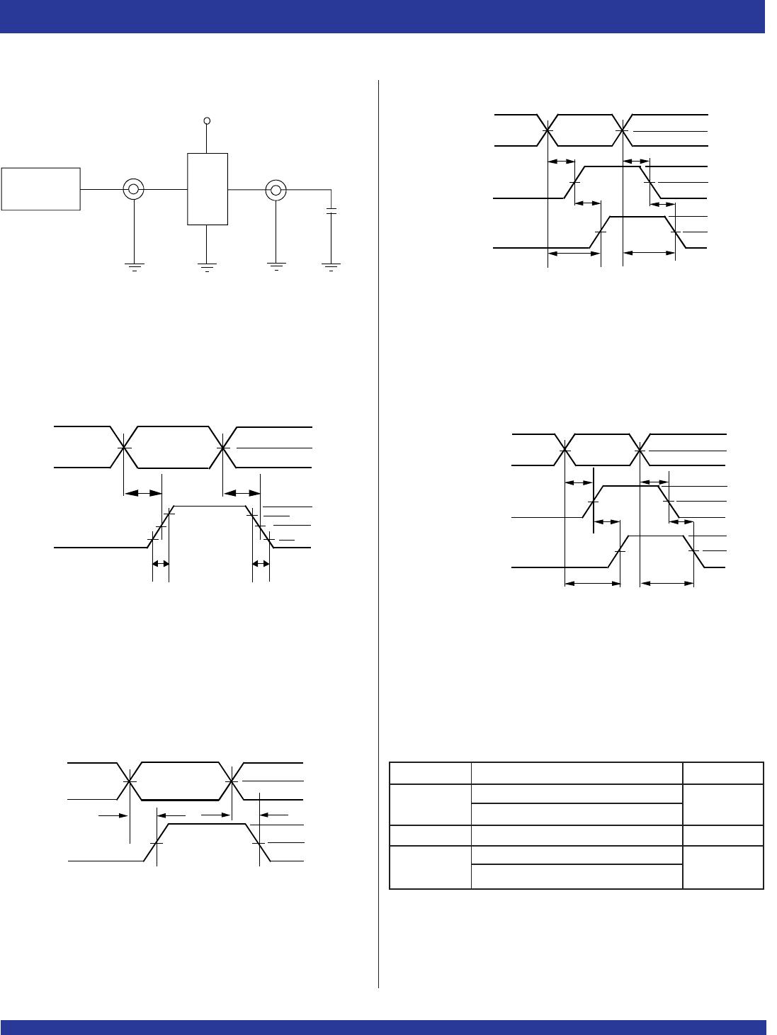
3. See test circuits and waveforms.
4. Skew measured between all outputs under identical transitions and load conditions.
5. Skew measured is difference between propagation delay times tPHL and tPLH of same output under identical load conditions.
6. Part to part skew for all outputs given identical transitions and load conditions at identical VCC levels and temperature.
7. Airflow of 1m/s is recommended for frequencies above 133MHz.
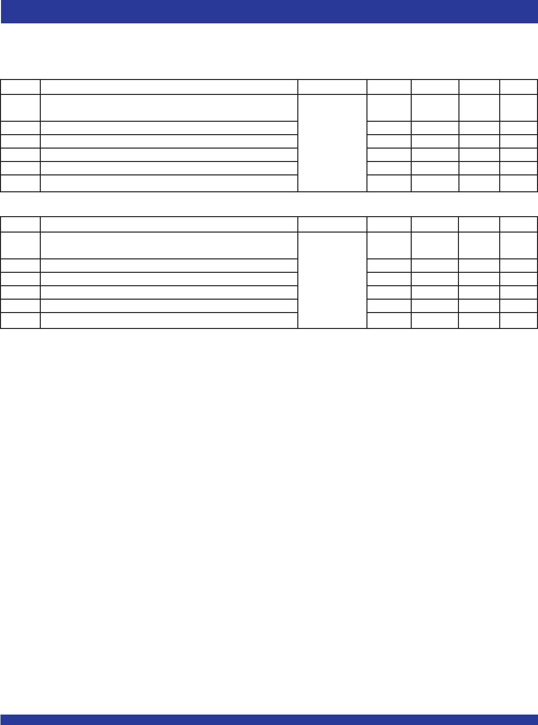
SWITCHING CHARACTERISTICS OVER OPERATING RANGE
(1,2)
Following Conditions Apply Unless Otherwise Specified
Industrial: TA = -40°C to +85°C, VCC = 2.5V ± 0.2V
Symbol Parameter Conditions
(3,7)
Min. Typ. Max. Unit
t
PLH Propagation Delay CL = 12pF 2.4 2.7 ns
tPHL 150 MHz
tR Output Rise Time 1 1.2 ns
tF Output Fall Time 1 1.2 ns
tSK(O) Same Device Output Pin-to-Pin Skew
(4)
100 150 ps
tSK(P) Pulse Skew
(5)
250 300 ps
t
SK(PP) Part-to-Part Skew
(6)
400 600 ps
Symbol Parameter Conditions
(3)
Min. Typ. Max. Unit
t
PLH Propagation Delay CL = 22pF 3 3.5 ns
tPHL 100 MHz
tR Output Rise Time 1 1.25 ns
tF Output Fall Time 1 1.25 ns
tSK(O) Same Device Output Pin-to-Pin Skew
(4)
100 150 ps
tSK(P) Pulse Skew
(5)
250 300 ps
t
SK(PP) Part-to-Part Skew
(6)
400 600 ps
5
IDT74FCT20807
2.5V CMOS 1-TO-10 CLOCK DRIVER
INDUSTRIAL TEMPERATURE RANGE
tPLH1
OUTPUT 1
OUTPUT 2
tSK(o)
tPLH2
2.5V
0V
V
OH
1.25V
1.25V
V
OL
VOH
1.25V
V
OL
INPUT
tPHL1
tPHL2
tSK(o)
tSK(o) = |tPLH2 - tPLH1| or |tPHL2 - tPHL1|
2.5V
0V
VOH
tPLH tPHL
VOL
1.25V
1.25V
tR
tF
1.7V
0.7V
INPUT
OUTPUT
tPLH
tPHL
2.5V
0V
V
OH
1.25V
1.25V
V
OL
tSK(p) = |tPHL - tPLH|
INPUT
OUTPUT
INPUT
tPLH1
DEVICE 1 OUTPUT
DEVICE 2 OUTPUT
t
SK(t)
tPLH2
2.5V
0V
V
OH
1.25V
1.25V
V
OL
VOH
1.25V
V
OL
tPHL1
tPHL2
tSK(t)
tSK(t) = |tPLH2 - tPLH1| or |tPHL2 - tPHL1|
Pulse
Generator
V
IN
VOUT
VCC
CL
D.U.T.
TEST CIRCUITS AND WAVEFORMS
NOTE: Device 1 and device 2 are same package type and speed grade.
Pulse Skew - tSK(P)
Part-to-Part Skew - tSK(PP)
Propagation Delay
Output Skew - tSK(O)
CL = Load Capacitance: Includes Jig and Probe Capacitance
TEST CONDITIONS
Symbol VCC = 2.5V ±0.2V Unit
C
L 22
(1)
pF
12
(2)
RT ZOUT of pulse generator
tR / tF 1.25
(1)
ns
1.2
(2)
DEFINITIONS:
CL = Load capacitance: includes jig and probe capacitance.
RT = Termination resistance: should be equal to ZOUT of the Pulse Generator.
tR / tF = Rise/Fall time of the input stimulus from the Pulse Generator.
NOTES:
1. Test conditions at 100MHz.
2. Test conditions at 150MHz.
6
INDUSTRIAL TEMPERATURE RANGE
IDT74FCT20807
2.5V CMOS 1-TO-10 CLOCK DRIVER
ORDERING INFORMATION
IDT74FCT
Temp. Range
XXXX
Device Type
X
Package
20807 1-to-10 2.5V Clock Driver
PY
Q
QG
Shrink Small Outline IC
Quarter-size Small Outline IC
QSOP - Green
X
I Industrial (-40°C to +85°C)
CORPORATE HEADQUARTERS for SALES: for Tech Support:
6024 Silver Creek Valley Road 800-345-7015 or 408-284-8200 clockhelp@idt.com
San Jose, CA 95138 fax: 408-284-2775
www.idt.com
PYG

74FCT20807QGI

Mfr. #:
Manufacturer:
IDT
Description:
Clock Buffer 2.5V 1:5 CLK DRIVER
Lifecycle:
New from this manufacturer.
Delivery:
DHL FedEx Ups TNT EMS
Payment:
T/T Paypal Visa MoneyGram Western Union