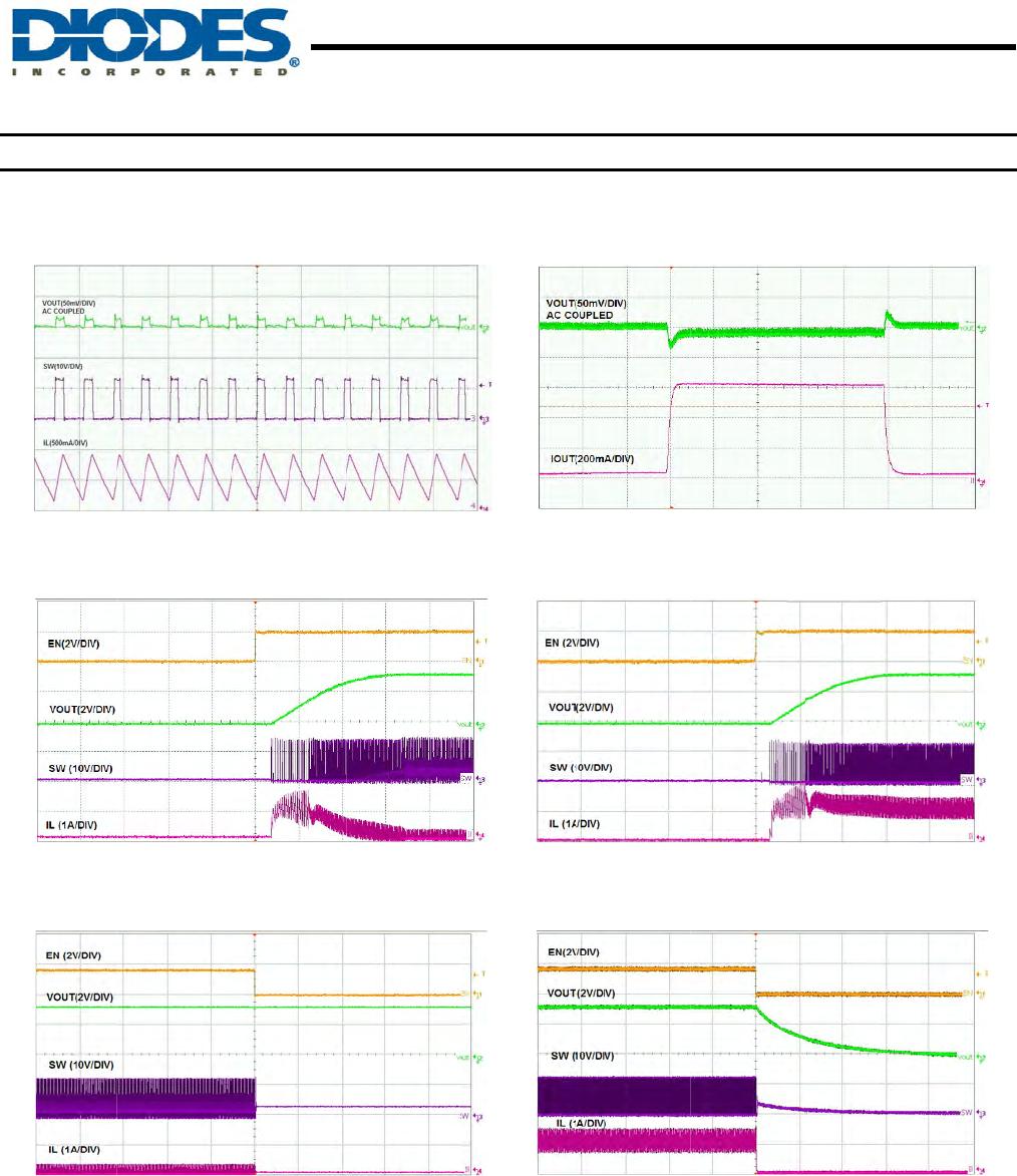
AP5100
1.2A STEP-DOWN CONVERTER with 1.4MHz SWITCHING
FREQUENCY
AP5100
Document number: DS32130 Rev. 3 - 2
4 of 12
www.diodes.com
April 2012
© Diodes Incorporated
Absolute Maximum Ratings (Note 2)
Symbol Description Rating Unit
ESD HBM Human Body Model ESD Protection 3 KV
ESD MM Machine Model ESD Protection 300 V
V
IN
Supply Voltage
26
V
V
SW
Switch Voltage
-0.3 to V
IN
+0.3
V
V
BST
Boost Voltage
V
SW
+6
V
All Other Pins –0.3 to +6 V
T
ST
Storage Temperature -65 to +150 °C
T
J
Junction Temperature +150 °C
T
L
Lead Temperature +260 °C
JA
Junction to Ambient Thermal Resistance (Note 3) 140 °C/W
JC
Junction to Case Thermal Resistance (Note 3) 35 °C/W
Notes: 2. Exceeding these ratings may damage the device.
3. Test condition for SOT26: Measured on approximately 1” square of 1 oz copper.
Recommended Operating Conditions (Note 4)
Symbol Description Rating Unit
V
IN
Supply Voltage 4.75 to 24 °C
T
A
Operating Ambient Temperature Range -25 to +85 °C
V
OUT
Output Voltage 0.81 to 15 V
Note: 4. The device function is not guaranteed outside of the recommended operating conditions.
AP5100
1.2A STEP-DOWN CONVERTER with 1.4MHz SWITCHING
FREQUENCY
AP5100
Document number: DS32130 Rev. 3 - 2
5 of 12
www.diodes.com
April 2012
© Diodes Incorporated
Electrical Characteristics (V
IN
= 12V, T
A
= +25°C, unless otherwise noted)
Note: 5. Guaranteed by design.
Symbol Parameter Test Conditions Min Typ. Max Unit
V
FB
Feedback Voltage
4.75V V
IN
24V
0.790 0.810 0.830 V
I
FB
Feedback Current
V
FB
= 0.8V
0.1 µA
R
DS(ON)
Switch-On Resistance (Note 5) 0.35
Switch Leakage
V
EN
= 0V, V
SW
= 0V
10 µA
Current Limit (Note 5) 2.4 A
f
SW
Oscillator Frequency
V
FB
= 0.6V
1.1 1.4 1.7 MHz
Fold-back Frequency
V
FB
= 0V
480 kHz
Maximum Duty Cycle
V
FB
= 0.6V
87 %
t
ON
Minimum On-Time (Note 5) 100 ns
Under Voltage Lockout Threshold
Rising
3.8 4.0 4.2 V
Under Voltage Lockout Threshold
Hysteresis
150 mV
EN Input Low Voltage 0.4 V
EN Input High Voltage 1.2 V
EN Input Current
V
EN
= 2V
0.3
µA
V
EN
= 0V
0.1
I
S
Supply Current (Shutdown)
V
EN
= 0V
0.1 1.0 µA
I
Q
Supply Current (Quiescent)
V
EN
= 2V, V
FB
= 1V
0.4 1.0 mA
Thermal Shutdown (Note 5) 140 °C
AP5100
Document numbe
r
Typical P
e
V
IN
= 12V, V
O
U
r
: DS32130 Rev. 3
e
rformanc
e
U
T
= 3.3V, L =
3
Stea
(I
O
Ti
m
Start-up
T
(
N
Tim
Shutdow
n
(
N
Tim
- 2
e
Charact
e
3
.3µH, C1 = 1
0
d
y State Test
UT
= 0.5A)
m
e- 1µs/div
T
hrough Ena
b
N
o Load)
e
- 50µs/div
n
Through En
a
N
o Load)
e
- 50µs/div
1.2A ST
E
w
e
ristics
0
µF, C2 = 22µ
F
b
le
a
ble
E
P-DOWN
C
6 of 12
w
ww.diodes.co
m
F
, T
A
= +25°C,
C
ONVER
T
m
unless other
w
L
o
(I
OUT
= 0.
2
Sta
r
(I
OU
T
Shut
d
(I
OU
T
T
ER with 1.
w
ise noted.
o
ad Transien
t
2
A to 0.8A. St
e
Time- 100µs/
d
r
t-up through
T
= 1A, resisti
v
Time- 50µs/
d
d
own Throug
h
T
= 1A, resisti
v
Time- 50µs/
d
A
P
4MHz SWI
FRE
Q
© Di
o
t
Test
e
p at 0.8A/µs)
d
iv
Enable
v
e load)
d
iv
h
Enable
v
e load)
d
iv
P
5100
TCHING
Q
UENCY
April 2012
o
des Incorporated

AP5100WG-7

Mfr. #:
Manufacturer:
Diodes Incorporated
Description:
Switching Voltage Regulators 1.2A Step-Down Conv 1.4MHz Sw Freq
Lifecycle:
New from this manufacturer.
Delivery:
DHL FedEx Ups TNT EMS
Payment:
T/T Paypal Visa MoneyGram Western Union

Products related to this Datasheet