AD8314
Rev. B | Page 18 of 20
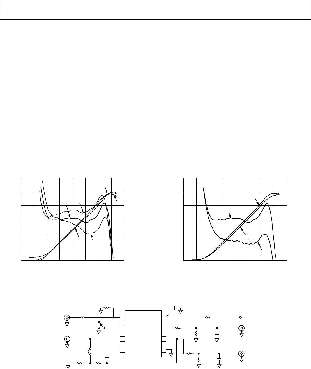
OPERATION AT 2.7 GHz
While the AD8314 is specified to operate at frequencies up to
2.5 GHz, it works at higher frequencies, although it does exhibit
slightly higher output voltage temperature drift.
Figure 43
shows the transfer function of a typical device at 2.7 GHz, at
ambient as well as hot and cold temperatures.
Figure 44 shows the transfer function of the AD8314 when
driven by both an unmodulated sine wave and a 64 QAM
signal. As previously discussed, the higher peak-to-average ratio
of the 64 QAM signal causes an increase in the intercept.
In this case, the intercept increases by approximately 1.5 dB,
causing the overall transfer function to drop by the same
amount. For precision operation, the AD8314 should be
calibrated for each signal type that is driving it.
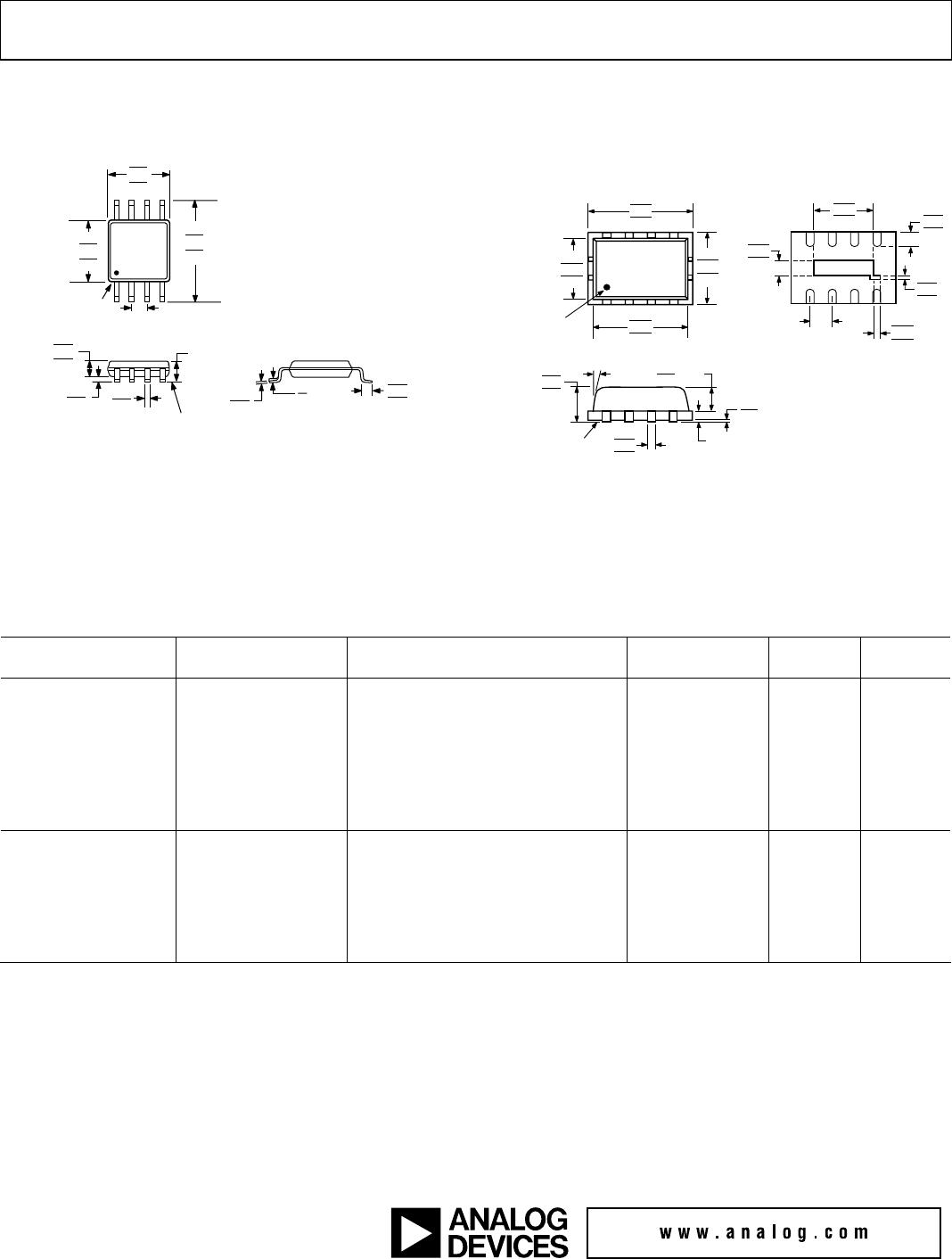
USING THE LFCSP PACKAGE
On the underside of the LFCSP package, there is an exposed,
compressed paddle. This paddle is internally connected to the
chip’s ground. While the paddle can be connected to the printed
circuit board’s ground plane, there is no thermal or electrical
requirement to do this.
EVALUATION BOARD
Figure 45 shows the schematic of the AD8314 MSOP
evaluation board. The layout and silkscreen of the component
side are shown in
Figure 46 and Figure 47. An evaluation board
is also available for the LFCSP package. (For exact part numbers,
see the
Ordering Guide.) Apart from the slightly smaller device
footprint, the LFCSP evaluation board is identical to the MSOP
board. The board is powered by a single supply in the 2.7 V to
5.5 V range. The power supply is decoupled by a single 0.1 µF
capacitor. Additional decoupling, in the form of a series resistor
or inductor in R9, can also be added.
Table 7 details the various
configuration options of the evaluation board.
1.2
0
–70 10
INPUT POWER (dBm)
V
UP
(V)
ERROR (dB)
3
–3
–2
–1
0
1
21.0
0.8
0.6
0.4
0.2
+25°C
–40°C
–40°C
+25°C
+80°C
+80°C
–60 –50 –40 –30 –20 –10 0
01086-043
Figure 43. Operating at 2.7 GHz
1.2
0
–70 10
INPUT POWER (dBm)
V
UP
(V)
ERROR (dB)
3
–3
–2
–1
0
1
21.0
0.8
0.6
0.4
0.2
–60 –50 –40 –30 –20 –10 0
CW
CW
64 QAM
64 QAM
01086-044
Figure 44. Shift in Transfer Function due to 64 QAM
V
POS
VSET
LK1
INPUT
SW1
V_DN
V_UP
VPOS
C1
0.1µF
1
2
3
4
ENBL
RFIN
AD8314
8
7
6
5
VSET
FLTR
V_DN
VPOS
COMM
V_UP
R2
52.3Ω
R1
0Ω
R7
0Ω
R8
OPEN
C4
(OPEN)
R4
(OPEN)
C2
(OPEN)
R6
(OPEN)
C3
(OPEN)
R3
0Ω
R5
0Ω
R9
0Ω
01086-045
Figure 45. Evaluation Board Schematic