© 2008 Microchip Technology Inc. DS22119A-page 1
24AA04H/24LC04BH
Device Selection Table
Features:
Single Supply with Operation Down to 1.7V for
24AA04H Devices, 2.5V for 24LC04BH Devices
Low-Power CMOS Technology:
- Read current 1 mA, max.
- Standby current 1 μA, max.
2-Wire Serial Interface, I
2
C™ Compatible
Schmitt Trigger Inputs for Noise Suppression
Output Slope Control to eliminate Ground Bounce
100 kHz and 400 kHz Clock Compatibility
Page Write Time 3 ms, typical
Self-Timed Erase/Write Cycle
16-Byte Page Write Buffer
Hardware Write-Protect for Half-Array (100h-1FFh)
ESD Protection >4,000V
More than 1 Million Erase/Write Cycles
Data Retention >200 years
Factory Programming available
Packages include 8-lead PDIP, SOIC, TSSOP,
TDFN, MSOP and 5-lead SOT-23
Pb-Free and RoHS Compliant
Temperature Ranges:
- Industrial (I): -40°C to +85°C
- Automotive (E): -40°C to +125°C
Description:
The Microchip Technology Inc. 24AA04H/24LC04BH
(24XX04H*) is an 4 Kbit Electrically Erasable PROM.
The device is organized as two blocks of 256 x 8-bit
memory with a 2-wire serial interface. Low-voltage
design permits operation down to 1.7V, with standby
and active currents of only 1 μA and 1 mA,
respectively. The 24XX04H also has a page write
capability for up to 16 bytes of data. The 24XX04H is
available in the standard 8-pin PDIP, surface mount
SOIC, TSSOP, 2x3 TDFN and MSOP packages, and
is also available in the 5-lead SOT-23 package. All
packages are Pb-free and RoHS compliant.
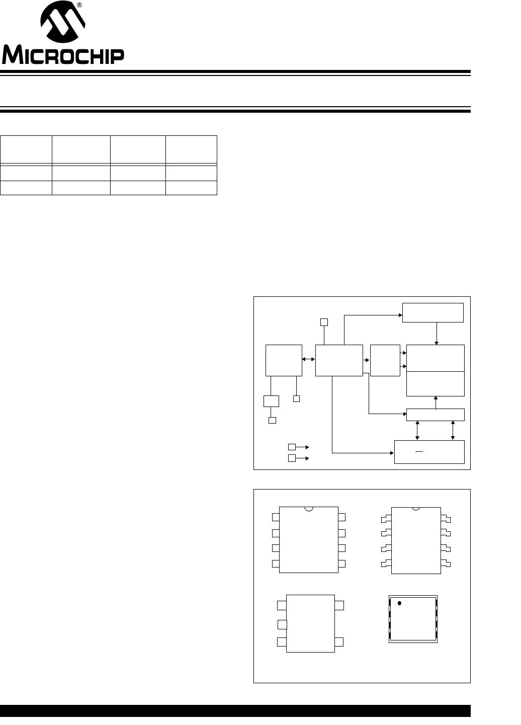
Block Diagram
Package Types
Part
Number
VCC
Range
Max. Clock
Frequency
Temp.
Ranges
24AA04H 1.7-5.5 400 kHz
(1)
I
24LC04BH 2.5-5.5 400 kHz I, E
Note 1: 100 kHz for VCC <2.5V
HV
EEPROM
Array
Page
YDEC
XDEC
Sense Amp.
Memory
Control
Logic
I/O
Control
Logic
I/O
WP
SDA
SCL
V
CC
VSS
R/W Control
Latches
Generator
A0
A1
A2
V
SS
VCC
WP
SCL
SDA
1
2
3
4
8
7
6
5
PDIP, MSOP
SOIC, TSSOP
A0
A1
A2
V
SS
1
2
3
4
8
7
6
5
V
CC
WP
SCL
SDA
TDFN
A0
A1
A2
V
SS
WP
SCL
SDA
V
CC
SOT-23-5
15
4
3
SCL
Vss
SDA
WP
Vcc
2
Note: Pins A0, A1 and A2 are not used by the 24XX04. (No
internal connections).
8
7
6
5
1
2
3
4
4K I
2
C
Serial EEPROM with Half-Array Write-Protect
*24XX04H is used in this document as a generic part
number for the 24AA04H/24LC04BH devices.
24AA04H/24LC04BH
DS22119A-page 2 © 2008 Microchip Technology Inc.
1.0 ELECTRICAL CHARACTERISTICS
Absolute Maximum Ratings
(†)
VCC.............................................................................................................................................................................6.5V
All inputs and outputs w.r.t. V
SS ......................................................................................................... -0.3V to VCC +1.0V
Storage temperature ...............................................................................................................................-65°C to +150°C
Ambient temperature with power applied................................................................................................-40°C to +125°C
ESD protection on all pins ......................................................................................................................................................≥ 4 kV
TABLE 1-1: DC CHARACTERISTICS
† NOTICE: Stresses above those listed under “Absolute Maximum Ratings” may cause permanent damage to
the device. This is a stress rating only and functional operation of the device at those or any other conditions
above those indicated in the operational listings of this specification is not implied. Exposure to maximum rating
conditions for extended periods may affect device reliability.
DC CHARACTERISTICS
V
CC = +1.7V to +5.5V
Industrial (I): T
A = -40°C to +85°C
Automotive (E): T
A = -40°C to +125°C
Param.
No.
Symbol Characteristic Min. Typ. Max. Units Conditions
D1 V
IH WP, SCL and SDA pins ——
D2 High-level input voltage 0.7 VCC ——V
D3 V
IL Low-level input voltage 0.3 VCC V—
D4 VHYS Hysteresis of Schmitt
Trigger inputs
0.05 VCC ——V(Note)
D5 V
OL Low-level output voltage 0.40 V IOL = 3.0 mA, VCC = 2.5V
D6 ILI Input leakage current ——±1μAVIN = VSS or VCC
D7 ILO Output leakage current ——±1μAVOUT = VSS or VCC
D8 CIN,
C
OUT
Pin capacitance
(all inputs/outputs)
——10pFVCC = 5.0V (Note)
T
A = 25°C, FCLK = 1 MHz
D9 ICC write Operating current —0.1 3mAVCC = 5.5V, SCL = 400 kHz
D10 I
CC read 0.05 1 mA
D11 ICCS Standby current
0.01
1
5
μA
μA
Industrial
Automotive
SDA = SCL = V
CC
WP = VSS
Note: This parameter is periodically sampled and not 100% tested.
© 2008 Microchip Technology Inc. DS22119A-page 3
24AA04H/24LC04BH
TABLE 1-2: AC CHARACTERISTICS
AC CHARACTERISTICS
Industrial (I): TA = -40°C to +85°C, VCC = +1.7V to +5.5V
Automotive (E): T
A = -40°C to +125°C, VCC = +2.5V to +5.5V
Param.
No.
Symbol Characteristic Min. Max. Units Conditions
1F
CLK Clock Frequency
400
100
kHz
kHz
2.5V VCC 5.5V
1.7V V
CC < 2.5V (24AA04H)
2 THIGH Clock High Time 600
4000
ns
ns
2.5V VCC 5.5V
1.7V V
CC < 2.5V (24AA04H)
3T
LOW Clock Low Time 1300
4700
ns
ns
2.5V VCC 5.5V
1.7V V
CC < 2.5V (24AA04H)
4TR SDA and SCL Rise Time
(Note 1)
300
1000
ns
ns
2.5V VCC 5.5V
1.7V V
CC < 2.5V (24AA04H)
5TF SDA and SCL Fall Time 300 ns (Note 1)
6THD:STA Start Condition Hold Time 600
4000
ns
ns
2.5V VCC 5.5V
1.7V V
CC < 2.5V (24AA04H)
7T
SU:STA Start Condition Setup Time 600
4700
ns
ns
2.5V VCC 5.5V
1.7V V
CC < 2.5V (24AA04H)
8T
HD:DAT Data Input Hold Time 0 ns (Note 2)
9TSU:DAT Data Input Setup Time 100
250
ns
ns
2.5V VCC 5.5V
1.7V V
CC < 2.5V (24AA04H)
10 T
SU:STO Stop Condition Setup Time 600
4000
ns
ns
2.5V VCC 5.5V
1.7V V
CC < 2.5V (24AA04H)
11 TSU:WP WP Setup Time 600
4000
ns
ns
2.5V VCC 5.5V
1.7V V
CC < 2.5V (24AA04H)
12 THD:WP WP Hold Time 1300
4700
ns
ns
2.5V VCC 5.5V
1.7V V
CC < 2.5V (24AA04H)
13 T
AA Output Valid from Clock
(Note 2)
900
3500
ns
ns
2.5V VCC 5.5V
1.7V V
CC < 2.5V (24AA04H)
14 TBUF Bus free time: Time the bus
must be free before a new
transmission can start
1300
4700
ns
ns
2.5V VCC 5.5V
1.7V V
CC < 2.5V (24AA04H)
15 T
OF Output Fall Time from VIH
Minimum to V
IL Maximum
250
250
ns
ns
2.5V V
CC 5.5V
1.7V V
CC < 2.5V (24AA04H)
16 T
SP Input Filter Spike Suppression
(SDA and SCL pins)
—50ns(Notes 1 and 3)
17 T
WC Write Cycle Time (byte or
page)
—5ms
18 Endurance 1M cycles 25°C, (Note 4)
Note 1: Not 100% tested. C
B = total capacitance of one bus line in pF.
2: As a transmitter the device must provide an internal minimum delay time to bridge the undefined region
(minimum 300 ns) of the falling edge of SCL to avoid unintended generation of Start or Stop conditions.
3: The combined T
SP and VHYS specifications are due to new Schmitt Trigger inputs which provide improved
noise spike suppression. This eliminates the need for a
TI specification for standard operation.
4: This parameter is not tested but ensured by characterization. For endurance estimates in a specific
application, please consult the Total Endurance™ Model which can be obtained on Microchip’s web site at
www.microchip.com.

24LC04BHT-I/OT

Mfr. #:
Manufacturer:
Microchip Technology
Description:
EEPROM 4K 512 X 8 2.5V SER EE IND 1/2 ARAY WP
Lifecycle:
New from this manufacturer.
Delivery:
DHL FedEx Ups TNT EMS
Payment:
T/T Paypal Visa MoneyGram Western Union