NLV74HC589ADTR2G

MC74HC589A
http://onsemi.com
4
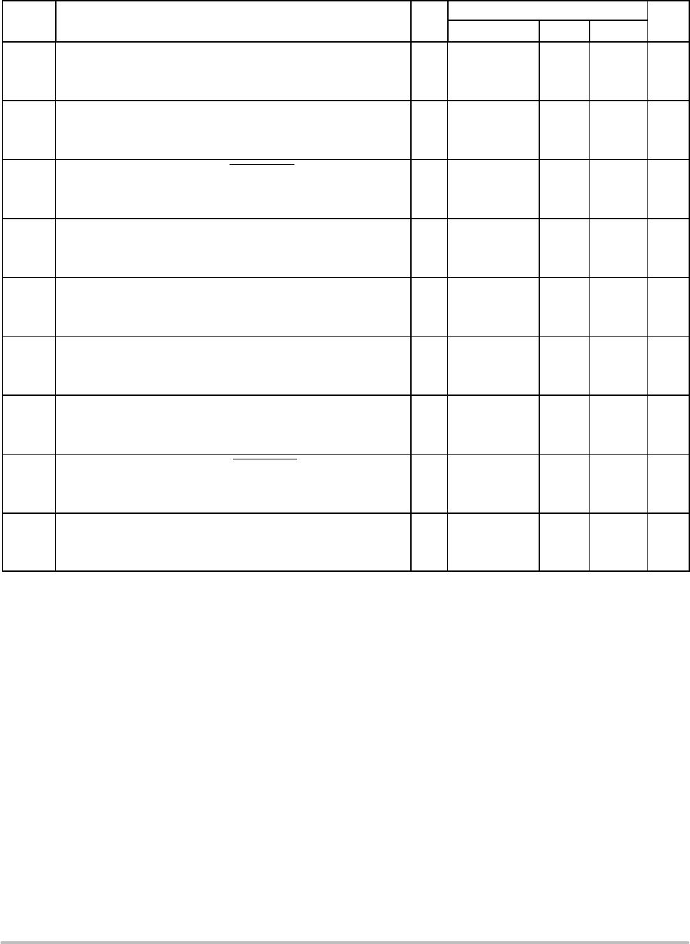
AC ELECTRICAL CHARACTERISTICS (C
L
= 50 pF, Input t
r
= t
f
= 6 ns)
V
CC
Guaranteed Limit
Symbol Parameter V
−55_C to 25_C 85_C 125_C
Unit
f
max
Maximum Clock Frequency (50% Duty Cycle)
(Figures 3 and9)
2.0
3.0
4.5
6.0
6.0
15
30
35
4.8
10
24
28
4.0
8.0
20
24
MHz
t
PLH
,
t
PHL
Maximum Propagation Delay, Latch Clock to Q
H
(Figures 2 and 9)
2.0
3.0
4.5
6.0
175
100
40
30
225
110
50
40
275
125
60
50
ns
t
PLH
,
t
PHL
Maximum Propagation Delay, Shift Clock to Q
H
(Figures 3 and 9)
2.0
3.0
4.5
6.0
160
90
30
25
200
130
40
30
240
160
48
40
ns
t
PLH
,
t
PHL
Maximum Propagation Delay, Serial Shift/Parallel Load to Q
H
(Figures 5 and 9)
2.0
3.0
4.5
6.0
160
90
30
25
200
130
40
30
240
160
48
40
ns
t
PLZ
,
t
PHZ
Maximum Propagation Delay, Output Enable to Q
H
(Figures 4 and 10)
2.0
3.0
4.5
6.0
150
80
27
23
170
100
30
25
200
130
40
30
ns
t
PZL
,
t
PZH
Maximum Propagation Delay, Output Enable to Q
H
(Figures 4 and 10)
2.0
3.0
4.5
6.0
150
80
27
23
170
100
30
25
200
130
40
30
ns
t
TLH
,
t
THL
Maximum Output Transition Time, Any Output
(Figures 2 and 9)
2.0
3.0
4.5
6.0
60
23
12
10
75
27
15
13
90
31
18
15
ns
C
in
Maximum Input Capacitance 10 10 10 pF
C
out
Maximum Three−State Output Capacitance
(Output in High−Impedance State)
15 15 15 pF
Typical @ 25_C, V
CC
= 5.0 V
C
PD
Power Dissipation Capacitance (per Package)* 50 pF
*Used to determine the no−load dynamic power consumption: P
D
= C
PD
V
CC
2
f + I
CC
V
CC
.
MC74HC589A
http://onsemi.com
5
TIMING REQUIREMENTS (Input t
r
= t
f
= 6 ns)
V
CC
Guaranteed Limit
Symbol Parameter V
−55_C to 25_C 85_C 125_C
Unit
t
su
Minimum Setup Time, A−H to Latch Clock
(Figure 6)
2.0
3.0
4.5
6.0
100
40
20
17
125
50
25
21
150
60
30
26
ns
t
su
Minimum Setup Time, Serial Data Input S
A
to Shift Clock
(Figure 7)
2.0
3.0
4.5
6.0
100
40
20
17
125
50
25
21
150
60
30
26
ns
t
su
Minimum Setup Time, Serial Shift/Parallel Load to Shift Clock
(Figure 8)
2.0
3.0
4.5
6.0
100
40
20
17
125
50
25
21
150
60
30
26
ns
t
h
Minimum Hold Time, Latch Clock to A−H
(Figure 6)
2.0
3.0
4.5
6.0
25
10
5
5
30
12
6
6
40
15
8
7
ns
t
h
Minimum Hold Time, Shift Clock to Serial Data Input S
A
(Figure 7)
2.0
3.0
4.5
6.0
5
5
5
5
5
5
5
5
5
5
5
5
ns
t
w
Minimum Pulse Width, Shift Clock
(Figure 3)
2.0
3.0
4.5
6.0
75
40
15
13
95
50
19
16
110
60
23
19
ns
t
w
Minimum Pulse Width, Latch Clock
(Figure 2)
2.0
3.0
4.5
6.0
80
40
16
14
100
50
20
17
120
60
24
20
ns
t
w
Minimum Pulse Width, Serial Shift/Parallel Load
(Figure 5)
2.0
3.0
4.5
6.0
80
40
16
14
100
50
20
17
120
60
24
20
ns
t
r
, t
f
Maximum Input Rise and Fall Times
(Figure 2)
2.0
3.0
4.5
6.0
1000
800
500
400
1000
800
500
400
1000
800
500
400
ns
MC74HC589A
http://onsemi.com
6
FUNCTION TABLE
Inputs Resulting Function
Operation
Output
Enable
Serial Shift/
Parallel Load
Latch
Clock
Shift
Clock
Serial
Input
S
A
Parallel
Inputs
A−H
Data
Latch
Contents
Shift
Register
Contents
Output
Q
H
Force Output into High
Impedance State
H X X X X X X X Z
Load Parallel Data into Data
Latch
L H L, H, X a−h a−h U U
Transfer Latch Contents to
Shift Register
L L L, H, X X X U LR
N
SR
N
LR
H
Contents of Input Latch and
Shift Register are Unchanged
L H
L, H,
L, H,
X X U U U
Load Parallel Data into Data
Latch and Shift Register
L L X X a−h a−h a−h h
Shift Serial Data into Shift
Register
L H X D X
*
SR
A
= D,
SR
N
SR
N+1
SR
G
SR
H
Load Parallel Data in Data
Latch and Shift Serial Data
into Shift Register
L H D a−h a−h SR
A
= D,
SR
N
SR
N+1
SR
G
SR
H
LR = latch register contents
SR = shift register contents
a−h = data at parallel data inputs A−H
D = data (L, H) at serial data input S
A
U = remains unchanged
X = don’t care
Z = high impedance
* = depends on Latch Clock input
90%
10%
Figure 2. (Serial Shift/Parallel Load = L) Figure 3. (Serial Shift/Parallel Load = H)
LATCH
CLOCK
Q
H
t
r
t
f
V
CC
GND
90%
50%
10%
t
PLH
t
PHL
t
TLH
t
THL
t
w
SHIFT
CLOCK
Q
H
V
CC
GND
50%
50%
t
PLH
t
PHL
1/f
max
90%
50%
10%
t
w
Figure 4.
Q
H
Q
H
50%
50%
t
PZL
t
PLZ
t
PZH
t
PHZ
V
CC
GND
HIGH
IMPEDANCE
V
OL
V
OH
OUTPUT
ENABLE
50%
SERIAL SHIFT/
PARALLEL LOAD
Q
H
50%
t
PLH
50%
V
CC
GND
t
PHL
50%
t
w
Figure 5.
SWITCHING WAVEFORMS
HIGH
IMPEDANCE

NLV74HC589ADTR2G

Mfr. #:
Manufacturer:
ON Semiconductor
Description:
Counter Shift Registers 8/BIT SHIFT REGISTER
Lifecycle:
New from this manufacturer.
Delivery:
DHL FedEx Ups TNT EMS
Payment:
T/T Paypal Visa MoneyGram Western Union