Semiconductor Components Industries, LLC, 2010
October, 2010 -- Rev. 4
1 Publication Order Number:
NB2760A/D
NB2760A
Low Power, Reduced EMI
Clock Synthesizer
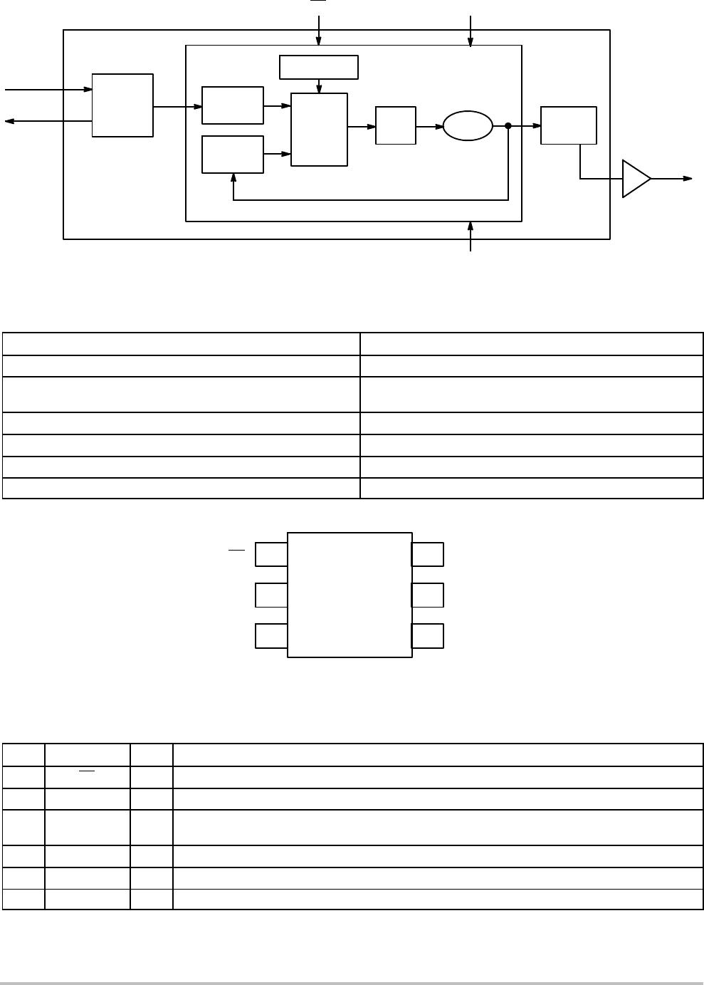
The NB2760A is a versatile spread spectrum frequency modulator
designed specifically for a wide range of clock frequencies. The
NB2760A reduces ElectroMagnetic Interference (EMI) at the clock
source, allowing system wide reduction of EMI of all clock dependent
signals. The NB2760A allows significant system cost savings by
reducing the number of circuit board layers, ferrite beads and
shielding that are traditionally required to pass EMI regulations.
The NB2760A uses the most efficient and optimized modulation
profile approved by the FCC and is implemented by using a
proprietary all digital method.
The NB2760A modulates the output of a single PLL in order to
“spread” the bandwidth of a synthesized clock, and more importantly,
decreases the peak amplitudes of its harmonics. This results in
significantly lower system EMI compared to the typical narrow band
signal produced by oscillators and most frequency generators.
Lowering EMI by increasing a signal’s bandwidth is called ‘spread
spectrum clock generation’.
The NB2760A is targeted towards all portable devices with very
low power requirements like MP3 players and digital still cameras.
Features
Generates an EMI Optimized Clocking Signal at the Output
Integrated Loop Filter Components
Operates with a 3.3 V / 2.5 V Supply
Operating Current less than 4.0 mA
Low Power CMOS Design
Input Frequency Range: 6.0 MHz to 12 MHz for 2.5 V
Input Frequency Range: 6.0 MHz to 13 MHz for 3.3 V
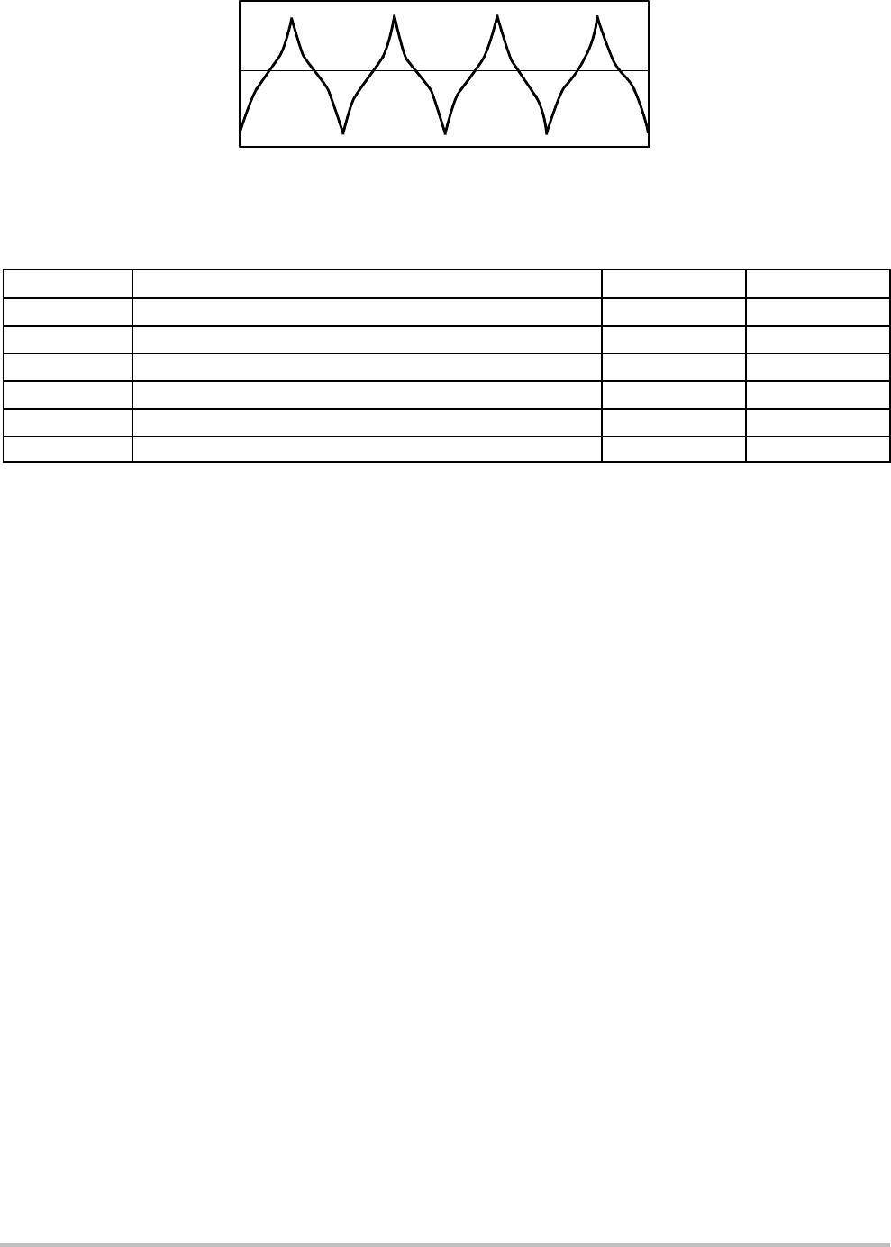
Generates a 1X Low EMI Spread Spectrum clock of the Input
Frequency
Frequency Deviation 0.65% @ 8 MHz
Available in TSOP--6 Package (TSOT--23--6)
Pb--Free Package is Available
1
6
*For additional marking information, refer to
sApplication Note AND8002/D.
TSOP--6
(TSOT--23--6)
SN SUFFIX
CASE 318G
See detailed ordering and shipping informationin the package
dimensions section on page 7 of this data sheet.
ORDERING INFORMATION
http://onsemi.com
MARKING
DIAGRAM*
E03 = Specific Device Code
A =Assembly Location
Y = Year
W = Work Week
G = Pb --Free Package
(Note: Microdot may be in either location)
E03AYWG
G
1