Data Sheet OP282/OP482
Rev. I | Page 13 of 16
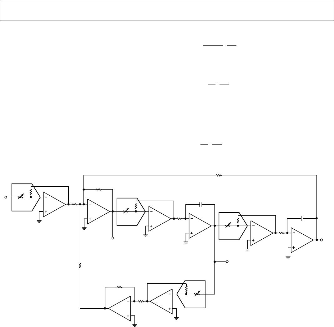
PROGRAMMABLE STATE VARIABLE FILTER
The circuit shown in Figure 48 can be used to accurately
program the Q, the cutoff frequency (f
C
), and the gain of a two-
pole state variable filter. OP482 devices have been used in this
design because of their high bandwidths, low power, and low
noise. This circuit takes only three packages to build because of
the quad configuration of the op amps and DACs.
The DACs shown are used in the voltage mode; therefore, many
values are dependent on the accuracy of the DAC only and not
on the absolute values of the DAC’s resistive ladders. This
makes this circuit unusually accurate for a programmable filter.
Adjusting DAC 1 changes the signal amplitude across R1; therefore,
the DAC attenuation times R1 determines the amount of signal
current that charges the integrating capacitor, C1.
This cutoff frequency can now be expressed as
=
256
2
π
1 D1
R1C1
f
C
where D1 is the digital code for the DAC.
The gain of this circuit is set by adjusting D3. The gain equation is
=
256
D3
R5
R4
Gain
DAC 2 is used to set the Q of the circuit. Adjusting this DAC
controls the amount of feedback from the band-pass node to
the input summing node. Note that the digital value of the
DAC is in the numerator; therefore, zero code is not a valid
operating point.
=
D2R3
R2
Q
256
R5
2k
Ω
1/4
OP482
V
IN
1/4
DAC8408
HIGH PASS
C1
1000pF
R4
2k
Ω
R6
2k
Ω
R7
2k
Ω
1/4
OP482
R1
2k
Ω
1/4
OP482
1/4
DAC8408
1/4
OP482
R1
2k
Ω
1/4
OP482
1/4
DAC8408
1/4
OP482
C1
1000pF
LOW
PASS
1/4
OP482
1/4
OP482
1/4
DAC8408
BAND PASS
R2
2k
Ω
R3
2k
Ω
00301-047
Figure 48. Programmable State Variable Filter