SI2324DS-T1-GE3

Vishay Siliconix
Si2324DS
Document Number: 67691
S12-1140-Rev. B, 21-May-12
www.vishay.com
1
This document is subject to change without notice.
THE PRODUCTS DESCRIBED HEREIN AND THIS DOCUMENT ARE SUBJECT TO SPECIFIC DISCLAIMERS, SET FORTH AT www.vishay.com/doc?91000
For technical questions, contact: pmostechsupport@vishay.com
N-Channel 100 V (D-S) MOSFET
FEATURES
•TrenchFET
®
Power MOSFET
100 % R
g
Tested
100 % UIS Tested
Material categorization:
For definitions of compliance please see
www.vishay.com/doc?99912
APPLICATIONS
DC/DC Converters
Load Switch
LED Backlighting in LCD TVs
Notes:
a. Based on T
C
= 25 °C.
b. Surface mounted on 1" x 1" FR4 board.
c. t = 5 s.
d. Maximum under steady state conditions is 166 °C/W.
MOSFET PRODUCT SUMMARY
V
DS
(V) R
DS(on)
()
I
D
(A)
a
Q
g
(Typ.)
100
0.234 at V
GS
= 10 V
2.3
2.9 nC
0.267 at V
GS
= 6 V
2.1
0.278 at V
GS
= 4.5 V
1.7
TO-236
(SOT-23)
Top View
Si2324DS (D4)*
* Marking Code
Ordering Information:
Si2324DS-T1-GE3 (Lead (Pb)-free and Halogen-free)
G
S
D
2
3
1
ABSOLUTE MAXIMUM RATINGS (T
A
= 25 °C, unless otherwise noted)
Parameter Symbol Limit Unit
Drain-Source Voltage
V
DS
100
V
Gate-Source Voltage
V
GS
± 20
Continuous Drain Current (T
J
= 150 °C)
T
C
= 25 °C
I
D
2.3
A
T
C
= 70 °C
1.8
T
A
= 25 °C
1.6
b, c
T
A
= 70 °C
1.3
b, c
Pulsed Drain Current (t = 300 µs)
I
DM
5
Continuous Source-Drain Diode Current
T
C
= 25 °C
I
S
2.1
T
A
= 25 °C
1.0
b, c
Single Pulse Avalanche Current
L = 0.1 mH
I
AS
5
Single Pulse Avalanche Energy
E
AS
1.25
mJ
Maximum Power Dissipation
T
C
= 25 °C
P
D
2.5
W
T
C
= 70 °C
1.6
T
A
= 25 °C
1.25
b, c
T
A
= 70 °C
0.8
b, c
Operating Junction and Storage Temperature Range
T
J
, T
stg
- 55 to 150
°C
THERMAL RESISTANCE RATINGS
Parameter Symbol Typical Maximum Unit
Maximum Junction-to-Ambient
b, d
5 s
R
thJA
75 100
°C/W
Maximum Junction-to-Foot (Drain)
Steady State
R
thJF
40 50
www.vishay.com
2
Document Number: 67691
S12-1140-Rev. B, 21-May-12
Vishay Siliconix
Si2324DS
This document is subject to change without notice.
THE PRODUCTS DESCRIBED HEREIN AND THIS DOCUMENT ARE SUBJECT TO SPECIFIC DISCLAIMERS, SET FORTH AT www.vishay.com/doc?91000
For technical questions, contact: pmostechsupport@vishay.com
Notes:
a. Pulse test; pulse width 300 µs, duty cycle 2 %.
b. Guaranteed by design, not subject to production testing.
Stresses beyond those listed under “Absolute Maximum Ratings” may cause permanent damage to the device. These are stress ratings only, and functional operation
of the device at these or any other conditions beyond those indicated in the operational sections of the specifications is not implied. Exposure to absolute maximum
rating conditions for extended periods may affect device reliability.
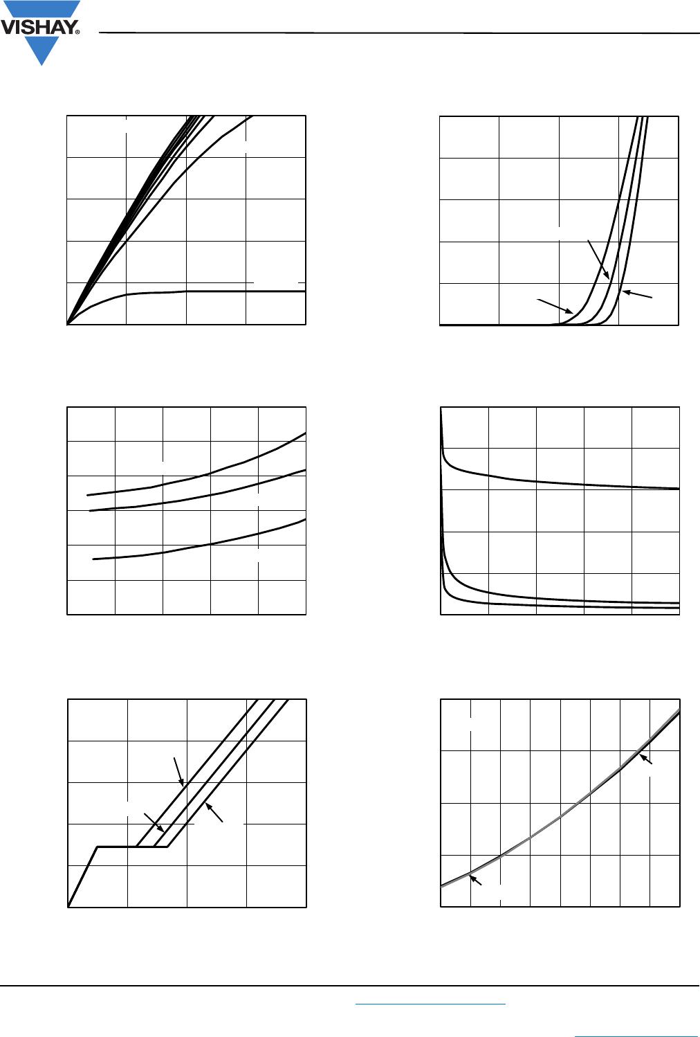
MOSFET SPECIFICATIONS (T
J
= 25 °C, unless otherwise noted)
Parameter Symbol Test Conditions Min. Typ. Max. Unit
Static
Drain-Source Breakdown Voltage
V
DS
V
DS
= 0 V, I
D
= 250 µA
100 V
V
DS
Temperature Coefficient V
DS
/T
J
I
D
= 250 µA
105
mV/°C
V
GS(th)
Temperature Coefficient
V
GS(th)
/T
J
- 5.2
Gate-Source Threshold Voltage
V
GS(th)
V
DS
= V
GS
, I
D
= 250 µA
1.2 2.8 V
Gate-Source Leakage
I
GSS
V
DS
= 0 V, V
GS
= ± 20 V
± 100 nA
Zero Gate Voltage Drain Current
I
DSS
V
DS
= 100 V, V
GS
= 0 V
- 1
µA
V
DS
= 100 V, V
GS
= 0 V, T
J
= 55 °C
- 10
On-State Drain Current
a
I
D(on)
V
DS
5 V, V
GS
= 4.5 V
5A
Drain-Source On-State Resistance
a
R
DS(on)
V
GS
= 10 V, I
D
= 1.5 A
0.195 0.234
V
GS
= 6 V, I
D
= 1 A
0.222 0.267
V
GS
= 4.5 V, I
D
= 0.5 A
0.231 0.278
Forward Transconductance
a
g
fs
V
DS
= 20 V, I
D
= 1.5 A
2.0 S
Dynamic
b
Input Capacitance
C
iss
V
DS
= 50 V, V
GS
= 0 V, f = 1 MHz
190
pFOutput Capacitance
C
oss
22
Reverse Transfer Capacitance
C
rss
13
Total Gate Charge
Q
g
V
DS
= 50 V, V
GS
= 10 V, I
D
= 1.6 A
5.2 10.4
nC
V
DS
= 50 V, V
GS
= 4.5 V, I
D
= 1.6 A
2.9 5.8
Gate-Source Charge
Q
gs
0.75
Gate-Drain Charge
Q
gd
1.4
Gate Resistance
R
g
f = 1 MHz 0.3 1.4 2.8
Tur n - O n D e l ay Time
t
d(on)
V
DD
= 50 V, R
L
= 39
I
D
= 1.3 A, V
GEN
= 4.5 V, R
g
= 1
30 45
ns
Rise Time
t
r
26 39
Turn-Off Delay Time
t
d(off)
17 26
Fall Time
t
f
12 20
Tur n - O n D e l ay Time
t
d(on)
V
DD
= 50 V, R
L
= 39
I
D
= 1.3 A, V
GEN
= 10 V, R
g
= 1
612
Rise Time
t
r
10 20
Turn-Off Delay Time
t
d(off)
10 20
Fall Time
t
f
612
Drain-Source Body Diode Characteristics
Continuous Source-Drain Diode Current
I
S
T
C
= 25 °C
- 2.1
A
Pulse Diode Forward Current
a
I
SM
- 20
Body Diode Voltage
V
SD
I
S
= 1.3 A
- 0.8 - 1.2 V
Body Diode Reverse Recovery Time
t
rr
I
F
= 1.3 A, dI/dt = 100 A/µs, T
J
= 25 °C
22 33 ns
Body Diode Reverse Recovery Charge
Q
rr
21 32 nC
Reverse Recovery Fall Time
t
a
16
ns
Reverse Recovery Rise Time
t
b
6
Document Number: 67691
S12-1140-Rev. B, 21-May-12
www.vishay.com
3
Vishay Siliconix
Si2324DS
This document is subject to change without notice.
THE PRODUCTS DESCRIBED HEREIN AND THIS DOCUMENT ARE SUBJECT TO SPECIFIC DISCLAIMERS, SET FORTH AT www.vishay.com/doc?91000
For technical questions, contact: pmostechsupport@vishay.com
TYPICAL CHARACTERISTICS (25 °C, unless otherwise noted)
Output Characteristics
On-Resistance vs. Drain Current and Gate Voltage
Gate Charge
0
1
2
3
4
5
00.511.52
I
D
- Drain Current (A)
V
DS
- Drain-to-Source Voltage (V)
V
GS
= 10 V thru 5 V
V
GS
= 3 V
V
GS
= 4 V
0.16
0.18
0.20
0.22
0.24
0.26
0.28
012345
R
DS(on)
- On-Resistance (Ω)
I
D
- Drain Current (A)
V
GS
= 6 V
V
GS
= 4.5 V
V
GS
= 10 V
0
2
4
6
8
10
0 1.5 3 4.5 6
V
GS
- Gate-to-Source Voltage (V)
Q
g
- Total Gate Charge (nC)
V
DS
= 80 V
V
DS
= 25 V
V
DS
= 50 V
I
D
= 1.6 A
Transfer Characteristics
Capacitance
On-Resistance vs. Junction Temperature
0
0.6
1.2
1.8
2.4
3
01234
I
D
- Drain Current (A)
V
GS
- Gate-to-Source Voltage (V)
T
C
= 25 °C
T
C
= - 55 °C
T
C
= 125 °C
0
60
120
180
240
300
0 20406080100
C - Capacitance (pF)
V
DS
- Drain-to-Source Voltage (V)
C
iss
C
oss
C
rss
0.4
0.85
1.3
1.75
2.2
- 50 - 25 0 25 50 75 100 125 150
R
DS(on)
-On-Resistance
(Normalized)
T
J
- Junction Temperature (°C)
I
D
= 1.5 A
V
GS
= 6 V
V
GS
= 10 V

SI2324DS-T1-GE3

Mfr. #:
Manufacturer:
Vishay / Siliconix
Description:
MOSFET 100V Vds 20V Vgs SOT-23
Lifecycle:
New from this manufacturer.
Delivery:
DHL FedEx Ups TNT EMS
Payment:
T/T Paypal Visa MoneyGram Western Union

Products related to this Datasheet