LTC3527/LTC3527-1
1
35271fc
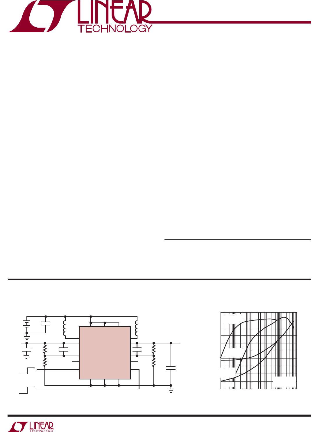
TYPICAL APPLICATION
LOAD CURRENT (mA)
30
EFFICIENCY (%)
POWER LOSS (mW)
90
100
20
10
80
50
70
60
40
0.01 1 10010 1000
35271 TA01b
0
1000
0.1
100
10
1
0.01
0.1
BURST
EFFICIENCY
FIXED
FREQUENCY
POWER
LOSS
BURST
V
IN
= 2.4V
V
OUT1
= 3.3V
FEATURES
APPLICATIONS
DESCRIPTION
Dual 800mA/400mA,
1.2MHz/2.2MHz Synchronous
Step-Up DC/DC Converters
The LTC
®
3527/LTC3527-1 are dual high effi ciency, step-up
DC/DC converters in a space saving 16-lead 3mm × 3mm
QFN package. Battery life is maximized with a 700mV start-
up voltage and operation down to 500mV once started.
The SHDN and PGOOD pins enable the converters to be
sequenced or started together.
The LTC3527/LTC3527-1 limit inrush current during start-
up. Selectable 1.2MHz or 2.2MHz operation provides a
choice between the highest effi ciency or smallest solu-
tion footprint. The current mode PWM design is internally
compensated reducing external parts count. Burst Mode
operation or fi xed frequency operation is selectable via the
MODE pin. Anti-ring circuitry reduces EMI in discontinuous
mode. This device also features thermal shutdown.
True output disconnect allows the output to be completely
open in shutdown. The LTC3527-1 actively discharges
V
OUT1
or V
OUT2
when its respective SHDN goes low. Qui-
escent current in shutdown is less than 2μA.
1.2MHz Effi ciency and Power Loss
n
Dual Synchronous Step-Up DC/DC Converters
n
Delivers 3.3V at 200mA/100mA from one Alkaline/
NiMH Cell, or 3.3V at 400mA/200mA from Two Cells
n
V
IN
Start-Up Voltage: 700mV
n
0.5V to 5V V
IN
Range After Start-Up
n
1.6V to 5.25V V
OUT
Range
n
Output Disconnect in Shutdown
n
V
IN
> V
OUT
Operation
n
1.2MHz or 2.2MHz Operation
n
Up to 94% Effi ciency
n
12μA Quiescent Current in Burst Mode
®
Operation
n
Inrush Current Limiting and Soft-Start
n
Internal Synchronous Rectifi ers
n
Logic-Controlled Shutdown (< 2μA)
n
Quick V
OUT
Discharge (LTC3527-1)
n
16-Lead, 0.75mm × 3mm × 3mm QFN Package
n
MP3/Personal Media Players
n
Noise Canceling/Bluetooth Headsets
n
Wireless Mice
n
Portable Medical Instruments
Two-Cell Alkaline to 3.3V/1.8V Synchronous Boost Converters
35271 TA01
+
ON
OFF
4.7μF
LTC3527
4.7μH 4.7μH
4.7
μF
4.7
μF
15pF 15pF
1.6V to 3.2V
SW1
V
OUT1
V
OUT2
V
IN1
V
IN
V
IN2
FB1
PGOOD1
SHDN1
SW2
FB2
PGOOD2
SHDN2
MODE GND F
SEL
V
OUT
3.3V
150mA
V
OUT
1.8V
150mA
V
IN
1.78M
1M
619k
1.21M
ON
OFF
L, LT, LTC, LTM, Linear Technology and the Linear logo are registered trademarks and
ThinSOT is a trademark of Linear Technology Corporation. All other trademarks are the
property of their respective owners.
LTC3527/LTC3527-1
2
35271fc
ELECTRICAL CHARACTERISTICS
PIN CONFIGURATIONABSOLUTE MAXIMUM RATINGS
V
IN
, V
IN1
, V
IN2
Voltage .................................0.3V to 6V
SW1, SW2 Voltage (DC) .............................. 0.3V to 6V
(Pulsed < 100ns) .....................................0.3V to 7V
SHDN1, SHDN2, FB1, FB2 Voltage ...............0.3V to 6V
V
OUT1
, V
OUT2
................................................0.3V to 6V
MODE, FSEL, PGOOD1, PGOOD2 .................0.3V to 6V
Operating Temperature (Notes 2, 5) .........40°C to 85°C
Junction Temperature ........................................... 125°C
Storage Temperature Range ...................65°C to 125°C
(Note 1)
16
17
PGND
15 14 13
5 6 7 8
TOP VIEW
UD PACKAGE
16-LEAD (3mm s 3mm) PLASTIC QFN
9
10
11
12
4
3
2
1SHDN1
FB1
MODE
V
IN1
SHDN
2
FB2
FSEL
V
IN2
PGOOD1
V
IN
GND
PGOOD2
V
OUT1
SW1
SW2
V
OUT2
T
JMAX
= 125°C, θ
JA
= 68°C/W
EXPOSED PAD (PIN 17) IS PGND, MUST BE SOLDERED TO PCB
PARAMETER CONDITIONS MIN TYP MAX UNITS
Minimum Start-Up Voltage I
LOAD
= 1mA 0.7 0.88 V
Output Voltage Adjust Range V
OUT1
V
OUT1
V
OUT2
V
OUT2
l
l
1.7
1.6
1.7
1.6
5.25
5.25
5.25
5.25
V
V
V
V
Line Regulation V
IN
= 1V to 5V 0.005 %/V
Feedback Voltage FB1, FB2
l
1.176 1.20 1.224 V
Feedback Input Current FB1, FB2 V
FB1,2
= 1.20V 1 50 nA
Quiescent Current: Shutdown V
SHDN1
= V
SHDN2
= 0V, Not Including Switch
Leakage, V
OUT1
= V
OUT2
= 0V
0.1 2 μA
Quiescent Current: Burst Mode Operation Measured on V
OUT
, V
FB1
= V
FB2
= 1.5V 12 μA
Quiescent Current: Active V
FB1
= V
FB2
> 1.2V (Note 3) 500 900 μA
NMOS Switch Leakage Current (LTC3527) V
SW1,2
= 5V, SHDN1,2 = 0V
0.1 10 μA
The l denotes the specifi cations which apply over the full operating
temperature range, –40°C to 85°C. V
IN
= V
IN1
= V
IN2
= 1.2V, V
OUT1
= V
OUT2
= 3.3V, T
A
= 25°C, unless otherwise noted.
ORDER INFORMATION
LEAD FREE FINISH TAPE AND REEL PART MARKING PACKAGE DESCRIPTION TEMPERATURE RANGE
LTC3527EUD#PBF LTC3527EUD#TRPBF LDDK
16-Lead (3mm × 3mm) Plastic QFN
–40°C to 85°C
LTC3527EUD-1#PBF LTC3527EUD-1#TRPBF LCXP
16-Lead (3mm × 3mm) Plastic QFN
–40°C to 85°C
LEAD BASED FINISH TAPE AND REEL PART MARKING PACKAGE DESCRIPTION TEMPERATURE RANGE
LTC3527EUD LTC3527EUD#TR LDDK
16-Lead (3mm × 3mm) Plastic QFN
–40°C to 85°C
LTC3527EUD-1 LTC3527EUD-1#TR LCXP
16-Lead (3mm × 3mm) Plastic QFN
–40°C to 85°C
Consult LTC Marketing for parts specifi ed with wider operating temperature ranges.
For more information on lead free part marking, go to:
http://www.linear.com/leadfree/
For more information on tape and reel specifi cations, go to:
http://www.linear.com/tapeandreel/
LTC3527/LTC3527-1
3
35271fc
ELECTRICAL CHARACTERISTICS
Note 1: Stresses beyond those listed under Absolute Maximum Ratings
may cause permanent damage to the device. Exposure to any Absolute
Maximum Rating condition for extended periods may affect device
reliability and lifetime.
Note 2: The LTC3527E/LTC3527E-1 are guaranteed to meet performance
specifi cations from 0°C to 85°C. Specifi cations over the –40°C to 85°C
operating temperature range are assured by design, characterization and
correlation with statistical process controls.
Note 3: Current is measured into the V
OUT
pin since the supply current is
bootstrapped to the output. The current will refl ect to the input supply by:
(V
OUT
/V
IN
) • (1/Effi ciency). All switches are off.
The l denotes the specifi cations which apply over the full operating
temperature range, –40
°C to 85°C. V
IN
= V
IN1
= V
IN2
= 1.2V, V
OUT1
= V
OUT2
= 3.3V, T
A
= 25°C, unless otherwise noted.
PARAMETER CONDITIONS MIN TYP MAX UNITS
PMOS Switch Leakage Current (LTC3527) V
SW1,2
= 5V, V
OUT1,2
= 0V, SHDN1,2 = 0V
0.1 10 μA
NMOS and PMOS Combined Switch Leakage Current
(LTC3527-1)
V
SW1,2
= 5V, V
OUT1,2
= 0V, SHDN1,2 = 0V (Note 6) 0.2 20 μA
NMOS Switch On-Resistance, SW1 0.30
Ω
NMOS Switch On-Resistance, SW2 0.50
Ω
PMOS Switch On-Resistance, SW1 0.40
Ω
PMOS Switch On-Resistance, SW2 0.60
Ω
NMOS Current Limit, SW1
l
800 mA
NMOS Current Limit, SW2
l
400 mA
Current Limit Delay to Output Time (Note 4) 60 ns
Maximum Duty Cycle V
FB1,2
= 1V
l
85 90 %
Minimum Duty Cycle V
FB1,2
= 1.3V
l
0%
Switching Frequency V
FSEL
= 0V
l
0.9 1.2 1.5 MHz
Switching Frequency V
FSEL
= 3.3V
l
1.8 2.2 2.8 MHz
SHDN1,2 Input High Voltage 0.88 V
SHDN1,2 Input Low Voltage 0.35 V
SHDN1,2 Input Current V
SHDN1,2
= 3.3V 1 2 μA
PGOOD1, PGOOD2 Threshold Referenced to the Feedback Voltage –6 –9 –14 %
PGOOD1, PGOOD2 Low Voltage I
PGOOD1,2
= 1mA 0.1 0.2 V
PGOOD1, PGOOD2 Leakage Current V
PGOOD1,2
= 5.25V 0.01 1 μA
MODE Input High Voltage 1V
MODE Input Low Voltage 0.35 V
MODE Input Current V
MODE
= 3.3V 1 2 μA
FSEL Input High Voltage 0.88 V
FSEL Input Low Voltage 0.35 V
FSEL Input Current V
FSEL
= 3.3V 1 2 μA
Soft-Start Time 0.5 ms
Note 4: Specifi cation is guaranteed by design and not 100% tested in
production.
Note 5: The LTC3527/LTC3527-1 includes an overtemperature shutdown
that is intended to protect the device during momentary overload
conditions. Junction temperature will exceed 125°C when the over-
temperature shutdown is active. Continuous operation above the specifi ed
maximum junction temperature may impair device reliability.
Note 6: The NMOS and PMOS switch leakage currents are tested in parallel
for the LTC3527-1 because V
OUT1,2
are actively pulled to ground when
SHDN1,2 = 0V

LTC3527EUD#TRPBF

Mfr. #:
Manufacturer:
Analog Devices / Linear Technology
Description:
Switching Voltage Regulators Dual 800mA/400mA, 1.2MHz/2.2MHz Synchronous Step-Up DC/DC Converters with Output Disconnect
Lifecycle:
New from this manufacturer.
Delivery:
DHL FedEx Ups TNT EMS
Payment:
T/T Paypal Visa MoneyGram Western Union