XC4VLX15-12FF676C

_______________General Description
The MAX4147 differential line driver offers high-speed
performance while consuming only 100mW of power.
Its amplifier has fully symmetrical inputs and outputs
and uses laser-trimmed, matched, thin-film resistors to
deliver 70dB CMR at 10MHz. Using current-feedback
techniques, the MAX4147 achieves a 300MHz band-
width and a 2000V/µs slew rate.
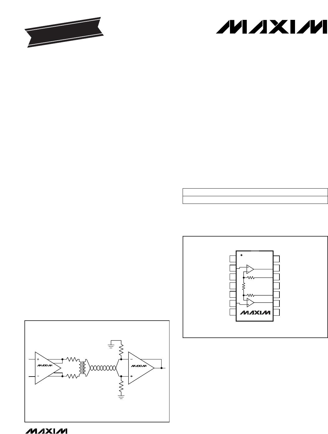
Optimized for differential, high-output-current applica-
tions such as transformer drivers, the MAX4147 drives
±2.6V into a 26.5load (single-ended) or ±5.6V into a
53 load (differential). This device is preset for a
closed-loop gain of 2V/V. Its ultra-low 0.008%/0.03° dif-
ferential gain/phase allow for a variety of video and RF
signal-processing applications.
For power-sensitive applications, the MAX4147 has a
shutdown function that reduces supply current to less
than 1mA. In addition, superior SFDR (-82dBc at
10kHz, R
L
= 33) makes it ideal as a transformer driver
for HDSL applications.
For a complete differential transmission link, use the
MAX4147 with the MAX4144 line receiver (see the
MAX4144 data sheet for more information).
________________________Applications
VDSL, ADSL, HDSL
Video Twisted-Pair Driver
Differential Pulse Amplifier
Differential ADC Driver
____________________________Features
2V/V Fixed Gain
300MHz -3dB Bandwidth
2000V/µs Slew Rate
82dBc SFDR at 10kHz
70dB CMR at 10MHz
Low Differential Gain/Phase: 0.008%/0.03°
High Output Drive: ±5.6V into 53
Low Power: 100mW
MAX4147
300MHz, Low-Power,
High-Output-Current, Differential Line Driver
________________________________________________________________
Maxim Integrated Products
1
14
13
12
11
10
9
8
1
2
3
4
5
6
7
V
CC
OUT+
SENSE+
GND
SHDN
N.C.
IN+
V
EE
TOP VIEW
MAX4147
SENSE-
OUT-
V
CC
V
EE
IN-
N.C.
SO
R
f
R
f
R
G
__________________Pin Configuration
MAX4144
MAX4147
OUT
OUT+
OUT-
IN-
IN+
IN-
IN+
SENSE
SENSE+
SENSE-
R
t
R
t
R
t
R
t
VDSL
TRANSFORMER ISOLATION
________Typical Application Circuit
19-1106; Rev 1; 11/96
PART
MAX4147ESD -40°C to +85°C
TEMP. RANGE PIN-PACKAGE
14 SO
EVALUATION KIT
AVAILABLE
______________Ordering Information
For free samples & the latest literature: http://www.maxim-ic.com, or phone 1-800-998-8800.
For small orders, phone 408-737-7600 ext. 3468.
MAX4147
300MHz, Low-Power,
High-Output-Current, Differential Line Driver
2 _______________________________________________________________________________________
ABSOLUTE MAXIMUM RATINGS
ELECTRICAL CHARACTERISTICS
(V
CC
= +5V, V
EE
= -5V, T
A
= T
MIN
to T
MAX
, unless otherwise noted. Typical values are at T
A
= +25°C.)
Stresses beyond those listed under “Absolute Maximum Ratings” may cause permanent damage to the device. These are stress ratings only, and functional
operation of the device at these or any other conditions beyond those indicated in the operational sections of the specifications is not implied. Exposure to
absolute maximum rating conditions for extended periods may affect device reliability.
Supply Voltage (V
CC
to V
EE
)..................................................12V
Voltage on Any Input to Ground ......(V
CC
+ 0.3V) to (V
EE
- 0.3V)
Continuous Power Dissipation (T
A
= +70°C)
SO (derate 8.33mW/°C above +70°C).........................667mW
Short-Circuit Duration.........................................................10sec
Operating Temperature Range
MAX4147ESD ..................................................-40°C to +85°C
Storage Temperature Range.............................-65°C to +160°C
Lead Temperature (soldering, 10sec).............................+300°C
V
OUT
= ±2.2V
V
OUT
= 0V, R
L
=
Differential, R
L
=
Single-ended, R
L
=
V
OUT
= 0V, R
L
=
V
IN
= 0, R
L
=
V
IN
= 0, R
L
=
V
S
= ±4.5V to ±5.5V
V
CM
= ±2.8V
f = 10kHz
V
OUT
= 0V, R
L
= , V
IN
= -V
OS
V
OUT
= 0V, R
L
= , V
IN
= -V
OS
R
L
=
CONDITIONS
V0.8V
IL
SHDN Low Threshold
V2.0V
IH
SHDN High Threshold
mA110 160I
OUT
Output Current Drive
7.2 7.8
3.2 3.8
mA0.6 1I
SHDN
Shutdown Supply Current
mA10 13I
SY
Quiescent Supply Current
dB70 100PSRPower-Supply Rejection
dB70 100CMRCommon-Mode Rejection
V/V
0.3 1
A
V
Gain 2
V-2.8 2.8V
CM
Common-Mode Input Voltage
Range
-3.6 3.6
µV/°C30TCV
OS
Input Offset Voltage Drift
mV0.5 6V
OS
Input Offset Voltage
M1Differential Input Resistance
pF1C
IN
Input Capacitance
1.7
µA9 20I
B
Input Bias Current
µA0.03 2I
OS
Input Offset Current
8
nV/Hz
80
e
n
Input Voltage Noise
UNITSMIN TYP MAXSYMBOLPARAMETER
f = 10kHz
f = 1MHz to 100MHz
R
L
=
-1V V
OUT
+1V, R
L
= 53
-1V V
OUT
+1V, R
L
= 53
V
SHDN
0.8V µA75 150
I
SHDN
SHDN Input Current
f = 1MHz to 100MHz
pA/Hz
17
I
n
Input Current Noise
Differential Input Voltage Range
V
Gain Error %
Differential, R
L
= 53
Single-ended, R
L
= 26.5
V
5.0 5.6
|
V
OUT
|
Output Voltage Swing
2.2 2.6
µV
RMS
nA
RMS
DC SPECIFICATIONS
V
SHDN
2V 10 nA
MAX4147
300MHz, Low-Power,
High-Output-Current, Differential Line Driver
_______________________________________________________________________________________ 3
ELECTRICAL CHARACTERISTICS (continued)
(V
CC
= +5V, V
EE
= -5V, T
A
= T
MIN
to T
MAX
, unless otherwise noted. Typical values are at T
A
= +25°C.)
CONDITIONS UNITSMIN TYP MAXSYMBOLPARAMETER
300
V
OUT
= 2Vp-p
V
OUT
0.1V
RMS
MHz
250
BW
(-3dB)
-3dB Bandwidth
f = 10MHz 70
70V
OUT
0.1V
RMS
MHzBW
(0.1dB)
0.1dB Bandwidth
f = 3.58MHz, R
L
= 150 0.008
Differential, -2V V
OUT
+2V 2000
f
C
= 5MHz, V
OUT
= 2Vp-p,
R
L
= 150differential, Figure 2
dBc
-75
SFDRSpurious-Free Dynamic Range
f
C
= 10kHz, V
OUT
= 4.0Vp-p, R
L
= 33single-
ended, R
S
= 50, Figure 1
-82
f = 3.58MHz, R
L
= 150 0.03
ns
10
t
s
Settling Time
1V V
OUT
+1V, R
L
= 150,
A
VCL
= +2
30
MHz
dB
V/µs
%
degrees
SRSlew Rate
DPDifferential Phase
DGDifferential Gain
CMRCommon-Mode Rejection
FPBWFull-Power Bandwidth
to 0.1%
to 0.01%
AC SPECIFICATIONS

XC4VLX15-12FF676C

Mfr. #:
Manufacturer:
Xilinx
Description:
FPGA - Field Programmable Gate Array
Lifecycle:
New from this manufacturer.
Delivery:
DHL FedEx Ups TNT EMS
Payment:
T/T Paypal Visa MoneyGram Western Union