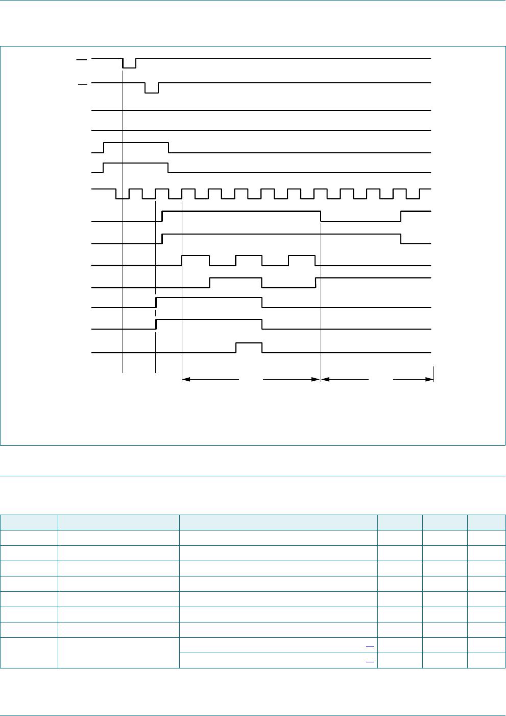
74HC161 All information provided in this document is subject to legal disclaimers. © NXP Semiconductors N.V. 2017. All rights reserved.
Product data sheet Rev. 3 — 4 January 2017 7 of 20
NXP Semiconductors
74HC161
Presettable synchronous 4-bit binary counter; asynchronous reset
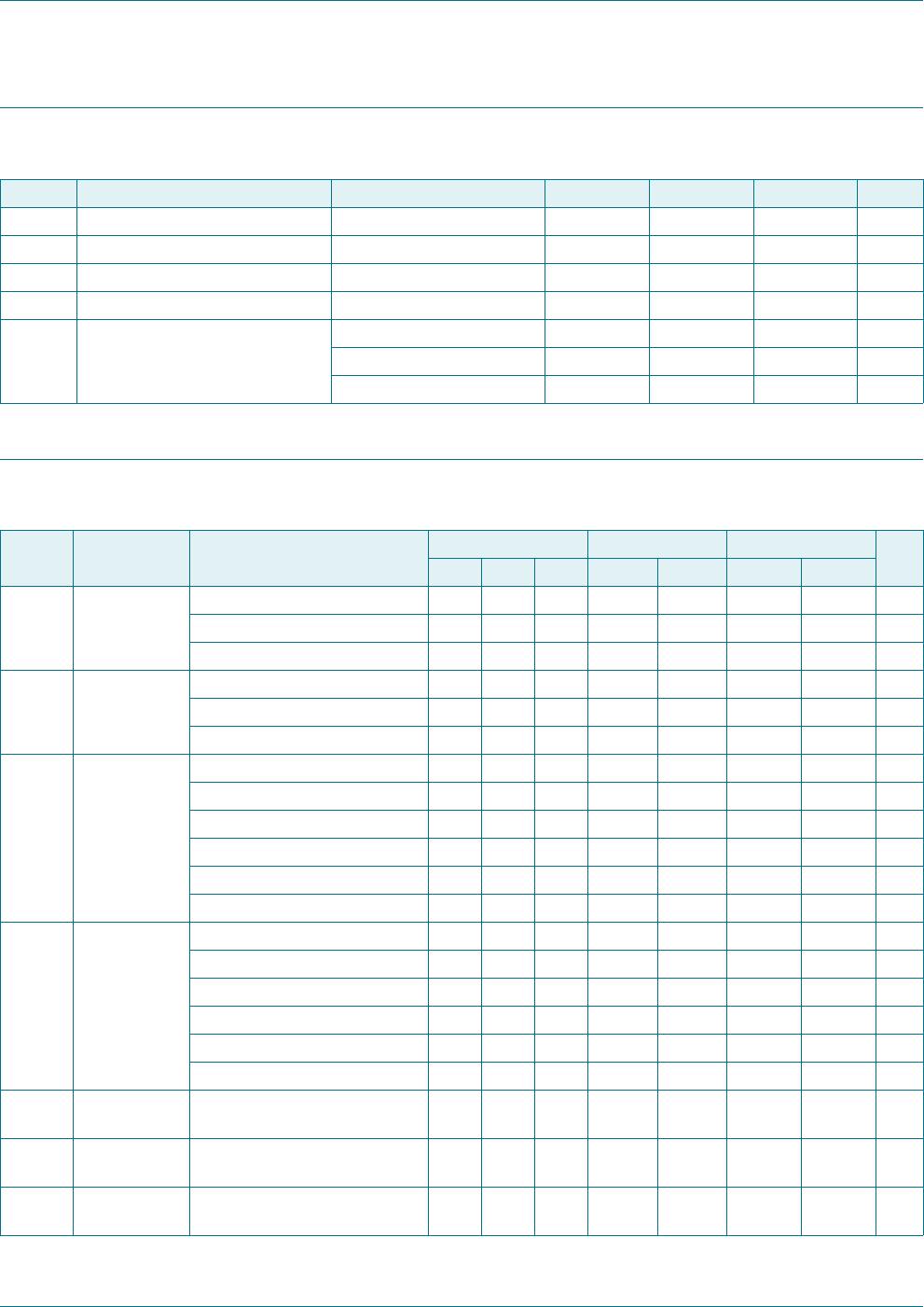
8. Recommended operating conditions
9. Static characteristics
Table 5. Recommended operating conditions
Voltages are referenced to GND (ground = 0 V)
Symbol Parameter Conditions Min Typ Max Unit
V
CC
supply voltage 2.0 5.0 6.0 V
V
I
input voltage 0 - V
CC
V
V
O
output voltage 0 - V
CC
V
T
amb
ambient temperature 40 +25 +125 C
t/V input transition rise and fall rate V
CC
= 2.0 V - - 625 ns/V
V
CC
= 4.5 V - 1.67 139 ns/V
V
CC
= 6.0 V - - 83 ns/V
Table 6. Static characteristics
At recommended operating conditions; voltages are referenced to GND (ground = 0 V).
Symbol Parameter Conditions 25 C 40 C to +85 C 40 C to +125 C Unit
Min Typ Max Min Max Min Max
V
IH
HIGH-level
input voltage
V
CC
= 2.0 V 1.5 1.2 - 1.5 - 1.5 - V
V
CC
= 4.5 V 3.15 2.4 - 3.15 - 3.15 - V
V
CC
= 6.0 V 4.2 3.2 - 4.2 - 4.2 - V
V
IL
LOW-level
input voltage
V
CC
= 2.0 V - 0.8 0.5 - 0.5 - 0.5 V
V
CC
= 4.5 V - 2.1 1.35 - 1.35 - 1.35 V
V
CC
= 6.0 V - 2.8 1.8 - 1.8 - 1.8 V
V
OH
HIGH-level
output voltage
V
I
=V
IH
or V
IL
I
O
= 20 A; V
CC
= 2.0 V 1.9 2.0 - 1.9 - 1.9 - V
I
O
= 20 A; V
CC
= 4.5 V 4.4 4.5 - 4.4 - 4.4 - V
I
O
= 20 A; V
CC
= 6.0 V 5.9 6.0 - 5.9 - 5.9 - V
I
O
= 4.0; V
CC
= 4.5 V 3.98 4.32 - 3.84 - 3.7 - V
I
O
= 5.2; V
CC
= 6.0 V 5.48 5.81 - 5.34 - 5.2 - V
V
OL
LOW-level
output voltage
V
I
=V
IH
or V
IL
I
O
=20A; V
CC
= 2.0 V - 0 0.1 - 0.1 - 0.1 V
I
O
=20A; V
CC
= 4.5 V - 0 0.1 - 0.1 - 0.1 V
I
O
=20A; V
CC
= 6.0 V - 0 0.1 - 0.1 - 0.1 V
I
O
=4.0mA; V
CC
= 4.5 V - 0.15 0.26 - 0.33 - 0.4 V
I
O
=5.2mA; V
CC
= 6.0 V - 0.16 0.26 - 0.33 - 0.4 V
I
I
input leakage
current
V
I
=V
CC
or GND; V
CC
=6.0V - - 0.1 - 1.0 - 1.0 A
I
CC
supply current V
I
=V
CC
or GND; I
O
=0A;
V
CC
=6.0V
- - 8.0 - 80.0 - 160.0 A
C
I
input
capacitance
-3.5- - - - -pF