BATTERY PROTECTION IC FOR 3-SERIAL- OR 4-SERIAL-CELL PACK
Rev.5.0_01
S-8254A Series
Seiko Instruments Inc.
15
5.
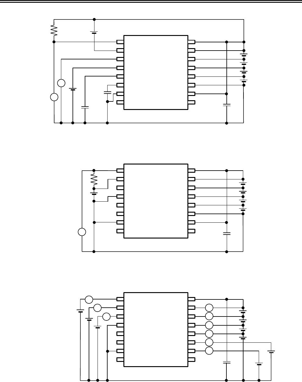
Overcurrent Status
The S-8254A Series has three overcurrent detection levels (V
IOV1
, V
IOV2
, and V
IOV3
) and three overcurrent
detection delay times (t
IOV1
, t
IOV2
, and t
IOV3
) corresponding to each overcurrent detection level. When the
discharging current becomes higher than the specified value (the voltage between V
SS
and V
INI
is greater
than V
IOV1
) and the state continues for t
IOV1
or longer, the S-8254A Series enters the overcurrent status, in
which the DOP pin voltage becomes V
DD
level to turn off the discharging FET to stop discharging, the
COP pin becomes high impedance and is pulled up to the EB+ pin voltage to turn off the charging FET to
stop charging, and the VMP pin is pulled up to the V
DD
voltage by the internal resistor (R
VMD
). Operation
of overcurrent detection level 2 (V
IOV2
) and overcurrent detection delay time 2 (t
IOV2
) is the same as for
V
IOV1
and t
IOV1
.
In the overcurrent status, the VMP pin is pulled up to the V
DD
level by the internal resistor in the IC (R
VMD
resistor). The overcurrent status is released when the following condition holds.
(1) The VMP pin voltage is V
IOV3
or higher because a charger is connected or the load (30 MΩ or
more) is released.
6. 0 V Battery Charge Function
Regarding the charging of a self-discharged battery (0 V battery), the S-8254A Series has two functions
from which one should be selected.
(1) 0 V battery charging is allowed (0 V battery charging is available.)
When the charger voltage is higher than V
0CHA
, the 0 V battery can be charged.
(2) 0 V battery charging is prohibited (0 V battery charging is unavailable.)
When one of the battery voltages is lower than V
0INH
, the 0 V battery cannot be charged.
Caution When the VDD pin voltage is lower than the minimum value of V
DSOP
, the operation of the
S-8254A Series is not guaranteed.
7. Delay Time Setting
The overcharge detection delay time (t
CU
) is determined by the external capacitor connected to the CCT
pin. The overdischarge detection delay time (t
DL
) and overcurrent detection delay time 1 (t
IOV1
) are
determined by the external capacitor connected to the CDT pin. Overcurrent detection delay times 2 and
3 (t
IOV2
, t
IOV3
) are fixed internally.
min. typ. max.
t
CU
[s] = (5.00, 10.0, 15.0) × C
CCT
[μF]
t
DL
[s] = (0.50, 1.00, 1.50) × C
CDT
[μF]
t
IOV1
[s] = (0.05, 0.10, 0.15) × C
CDT
[μF]
8. CTL Pin
The S-8254A Series has control pins. The CTL pin is used to control the COP and DOP pin output
voltages. CTL pin takes precedence over the battery protection circuit.
Table 5 Conditions Set by CTL Pin
CTL Pin COP Pin DOP Pin
High High-Z V
DD
Open High-Z V
DD
Low
Normal status
*1
Normal status
*1
*1. The status is controlled by the voltage detector.
Caution Please note unexpected behavior might occur when electrical potential difference
between the CTL pin (‘L’ level) and VSS is generated through the external filter
(R
VSS
and C
VSS
) as a result of input voltage fluctuations.