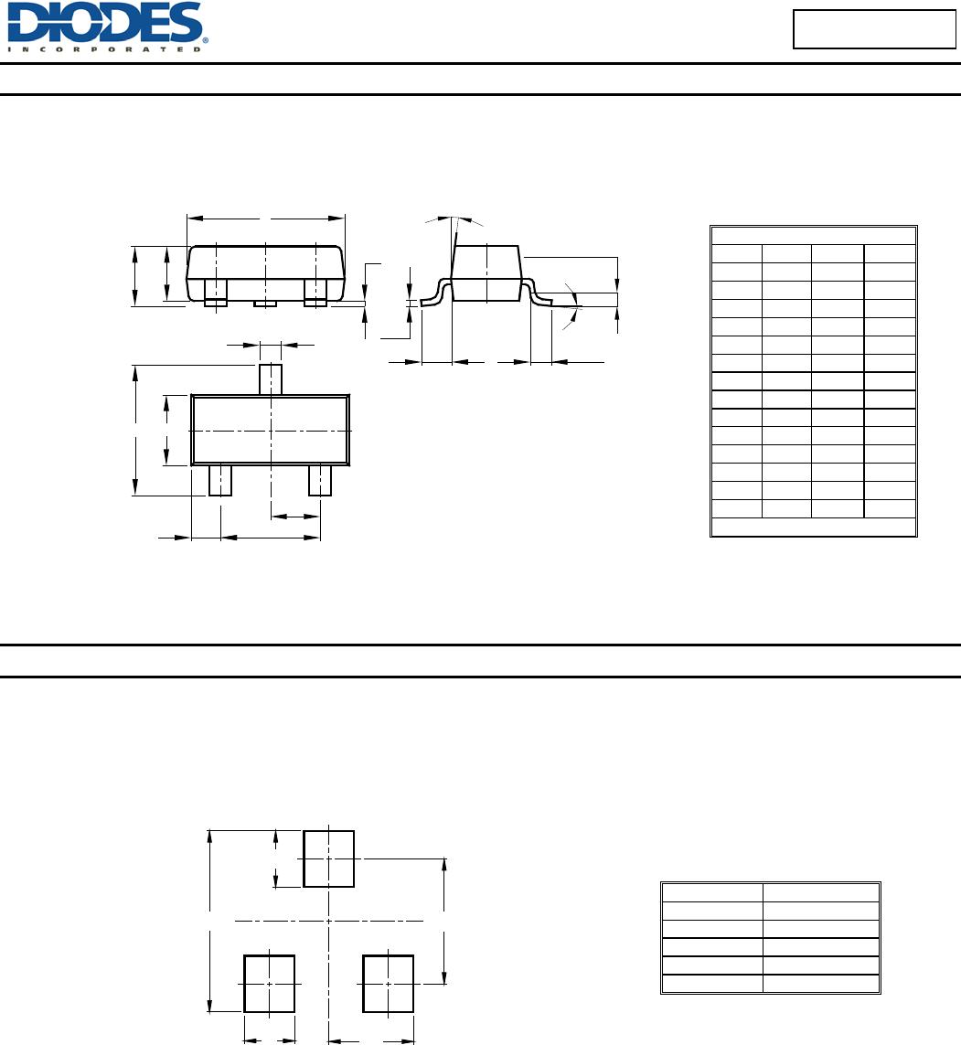
Document number: DS30041 Rev. 16 - 2
© Diodes Incorporated
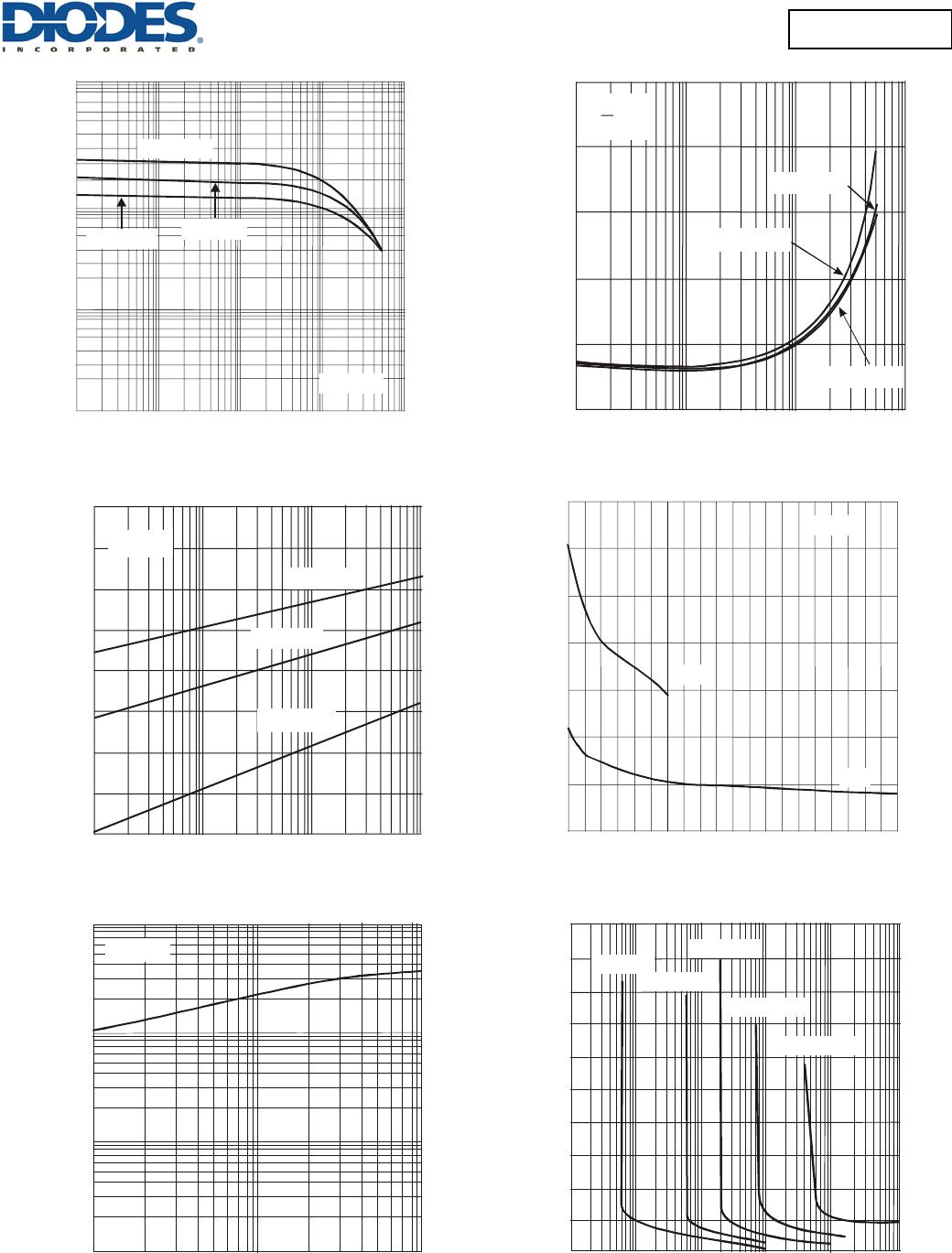
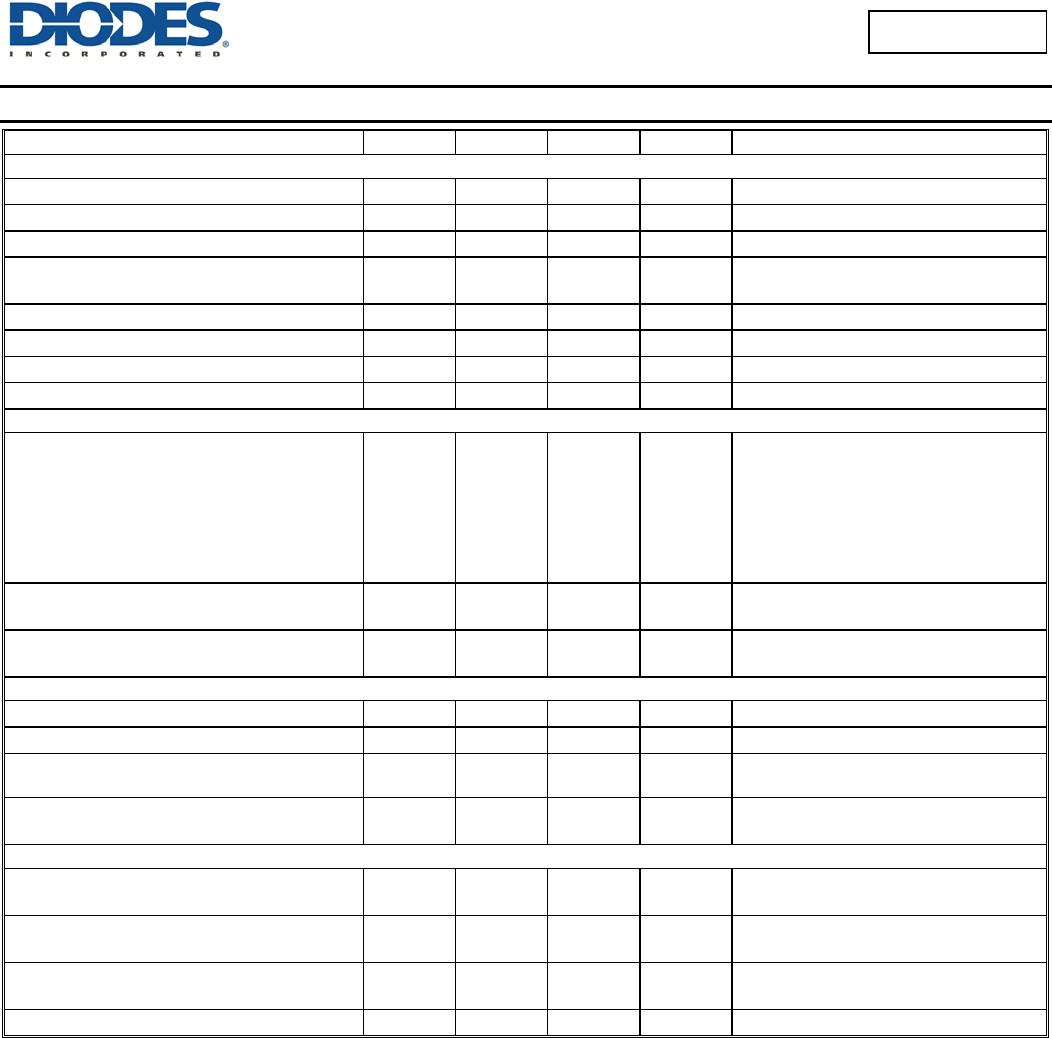
Electrical Characteristics (@T
A
= +25°C, unless otherwise specified.)
Collector-Base Breakdown Voltage
Collector-Emitter Breakdown Voltage (Note 10)
BV
40
V
I
= 10mA, I
= 0
Emitter-Base Breakdown Voltage
BV
6.0
V
I
= 100µA, I
= 0
Collector Cut-Off Current
I
CBO
10
nA
µA
V
CB
= 60V, I
E
= 0
V
CB
= 60V, I
E
= 0, T
A
= +150°C
Collector Cut-Off Current
10 nA
V
CE
= 60V, V
EB(OFF)
= 3.0V
Collector Cut-Off Current
V
CE
= 60V, V
BE
= ±0.25V
Base Cut-Off Current
I
BL
20 nA
V
CE
= 60V, V
EB(OFF)
= 3.0V
ON CHARACTERISTICS (Note 10)
DC Current Gain
h
FE
35
50
75
100
40
50
35
300
I
C
= 100µA, V
CE
= 10V
I
C
= 1.0mA, V
CE
= 10V
I
C
= 10mA, V
CE
= 10V
I
C
= 150mA, V
CE
= 10V
I
C
= 500mA, V
CE
= 10V
I
C
= 10mA, V
CE
= 10V, T
A
= -55°C
I
= 150mA, V
= 1.0V
Collector-Emitter Saturation Voltage
V
CE(SAT)
0.3
1.0
V
I
C
= 150mA, I
B
= 15mA
Base-Emitter Saturation Voltage
V
BE(SAT)
0.6
1.2
2.0
V
I
C
= 150mA, I
B
= 15mA
I
= 500mA, I
= 50mA
SMALL SIGNAL CHARACTERISTICS
Output Capacitance
C
obo
8 pF
V
CB
= 10V, f = 1.0MHz, I
E
= 0
Input Capacitance
C
— 25 pF
V
= 0.5V, f = 1.0MHz, I
= 0
Current Gain-Bandwidth Product
f
T
300
MHz
V
CE
= 20V, I
C
= 20mA,
Noise Figure
N
F
4.0 dB
V
CE
= 10V, I
C
= 100µA,
R
S
= 1.0kΩ,
f = 1.0kHz
SWITCHING CHARACTERISTICS
Delay Time
t
D
10 ns
V
CC
= 30V, I
C
= 150mA,
V
BE(OFF)
= - 0.5V, I
B1
= 15mA
Rise Time
t
R
25 ns
V
CC
= 3.0V, I
C
= 150mA, I
B1
= 15mA,
Storage Time
t
S
225 ns
V
CC
= 30V, I
C
= 150mA,
I
= I
= 15mA
V
CC
= 30V, I
C
= 150mA, I
B1
= I
B2
= 15mA
Note: 10. Measured under pulsed conditions. Pulse width ≤ 300µs. Duty cycle ≤ 2%.