LTC4353
9
4353f
MOSFET Selection
The LTC4353 drives N-channel MOSFETs to conduct the
load current. The important features of the MOSFET are
its maximum drain-source voltage BV
DSS
, maximum gate-
source voltage V
GS(MAX)
, and the on-resistance R
DS(ON)
.
If an input is connected to ground, the full supply voltage
can appear across the MOSFET. To survive this, the BV
DSS
must be higher than the supply voltages. The V
GS(MAX)
rating of the MOSFET should exceed 14V since that is
the upper limit of the internal GATE to V
IN
clamp. The
R
DS(ON)
of the MOSFET dictates the maximum voltage drop
(I
L
• R
DS(ON)
) and the power dissipated (I
L
2
• R
DS(ON)
)
in the MOSFET. Note that the minimum MOSFET voltage
drop is controlled by the servo amplifier regulation volt-
age, hence, picking a very low R
DS(ON)
(below V
FR
/I
L
) may
not be beneficial.
CPO Capacitor Selection
The recommended value of the capacitor between the CPO
and V
IN
pins is approximately 10× the input capacitance
C
ISS
of the MOSFET. A larger capacitor takes a cor-
respondingly longer time to be charged by the internal
charge pump. A smaller
capacitor suffers more voltage
drop
during a fast gate turn-on event as it shares charge
with the MOSFET gate capacitance.
External CPO Supply
The internal charge pump takes milliseconds to charge
up the CPO capacitor especially during device power-up.
This time can be shortened by connecting an external
supply to the CPO pin. A series resistor is needed to limit
the current into the internal clamp between CPO and V
IN
pins. The CPO supply should also be higher than the
main input supply to meet the gate drive requirements
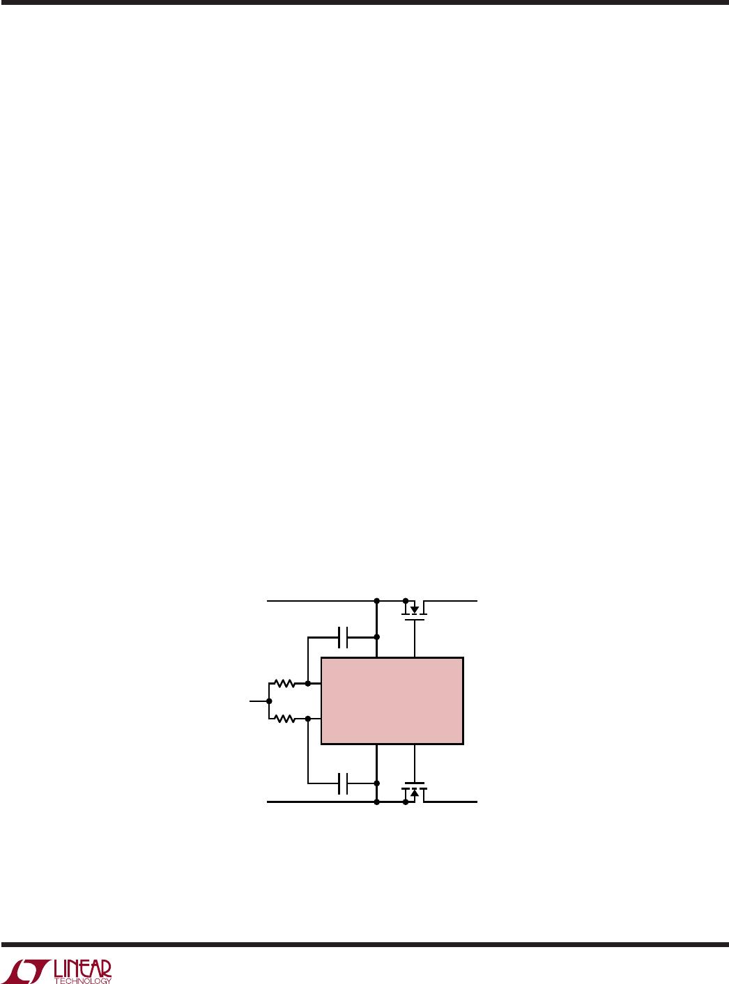
of the MOSFET. Figure 3 shows such a 3.3V ideal diode
application, where a 12V supply is connected to the CPO
pins through a 1k resistor. The 1k limits the current into
the CPO pin, when the V
IN
pin is grounded. For the 8.7V
gate drive (12V – 3.3V), logic-level MOSFETs would be an
appropriate choice for M1 and M2.
Input Transient Protection
When the capacitances at the input and output are very
small, rapid changes in current can cause transients that
exceed the 24V absolute maximum rating of the V
IN
and
OUT pins. In ORing applications, one surge suppressor
connected from OUT to ground clamps all the inputs.
In
the
absence of a surge suppressor, an output capacitance
of 10μF is sufficient in most applications to prevent the
transient from exceeding 24V.
Figure 3. 3.3V Ideal Diode with External 12V Supply
Powering CPO for Faster Start-Up and Refresh
M1
M2
GATE1
4353 F03
V
INA
3.3V
V
INB
3.3V
V
IN1
GATE2
V
IN2
LTC4353
CPO1
CPO2
12V
1k
1k
C1
56nF
C2
56nF
applicaTions inForMaTion