TSOP75433WTR

TSOP752..W, TSOP754..W
www.vishay.com
Vishay Semiconductors
Rev. 1.6, 22-Jul-16
4
Document Number: 82496
THIS DOCUMENT IS SUBJECT TO CHANGE WITHOUT NOTICE. THE PRODUCTS DESCRIBED HEREIN AND THIS DOCUMENT
ARE SUBJECT TO SPECIFIC DISCLAIMERS, SET FORTH AT www.vishay.com/doc?91000
Fig. 9 - Sensitivity vs. Ambient Temperature
Fig. 10 - Relative Spectral Sensitivity vs. Wavelength
Fig. 11 - Horizontal Directivity
Fig. 12 - Vertical Directivity
Fig. 13 - Sensitivity vs. Supply Voltage
0
0.1
0.2
0.3
0.4
0.5
0.6
-30 -10 10 30 50 70 90
E
e min.
- Threshold Irradiance (mW/m
2
)
T
amb
- Ambient Temperature (°C)
0
0.1
0.2
0.3
0.4
0.5
0.6
0.7
0.8
0.9
1.0
750 800 850 900 950 1000 1050 1100 1150
21425 λ- Wavelength (nm)
S (λ)
rel
- Relative Spectral Sensitivity
d
rel
- Relative Transmission Distance
21581
0.6 0.4 0.2 0
0.9
0.8
30°
10° 20°
40°
50°
60°
70°
80°
0.7
1.0
d
rel
- Relative Transmission Distance
21580
0.6 0.4 0.2 0
0.9
0.8
30°
10° 20°
40°
50°
60°
70°
80°
0.7
1.0
0.00
0.10
0.20
0.30
0.40
0.50
0.60
1 2 3 4 5
E
e min.
- Sensitivity (mW/m
2
)
V
S
- Supply Voltage (V)
TSOP752..W, TSOP754..W
www.vishay.com
Vishay Semiconductors
Rev. 1.6, 22-Jul-16
5
Document Number: 82496
THIS DOCUMENT IS SUBJECT TO CHANGE WITHOUT NOTICE. THE PRODUCTS DESCRIBED HEREIN AND THIS DOCUMENT
ARE SUBJECT TO SPECIFIC DISCLAIMERS, SET FORTH AT www.vishay.com/doc?91000
SUITABLE DATA FORMAT
This series is designed to suppress spurious output pulses
due to noise or disturbance signals. The devices can
distinguish data signals from noise due to differences in
frequency, burst length, and envelope duty cycle. The data
signal should be close to the device’s band-pass center
frequency (e.g. 38 kHz) and fulfill the conditions in the table
below.
When a data signal is applied to the product in the
presence of a disturbance, the sensitivity of the receiver is
automatically reduced by the AGC to insure that no spurious
pulses are present at the receiver’s output.
Some examples which are suppressed are:
DC light (e.g. from tungsten bulbs sunlight)
Continuous signals at any frequency
• Strongly or weakly modulated patterns from fluorescent
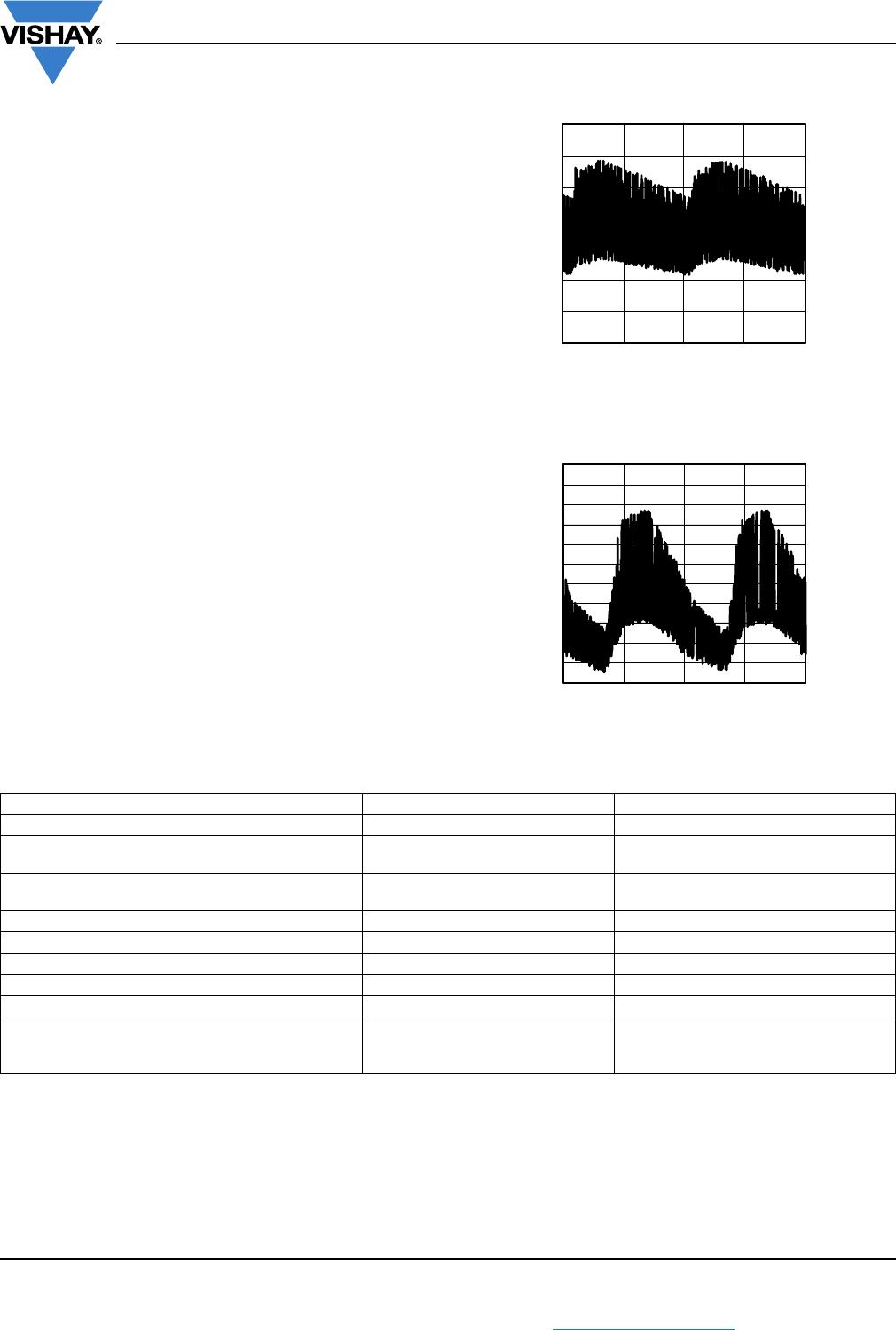
lamps with electronic ballasts (see Fig. 14 or Fig. 15)
Fig. 14 - IR Disturbance from Fluorescent Lamp
with Low Modulation
Fig. 15 - IR Disturbance from Fluorescent Lamp
with High Modulation
Notes
For data formats with short bursts please see the datasheet for TSOP753..W
For Sony 12, 15, and 20 bit IR codes please see the datasheet of TSOP75S40FW
0101520
Time (ms)
16920
IR Signal
5
0101520
Time (ms)
16921
IR Signal
5
TSOP752..W TSOP754..W
Minimum burst length 10 cycles/burst 10 cycles/burst
After each burst of length
a minimum gap time is required of
10 to 70 cycles
10 cycles
10 to 35 cycles
10 cycles
For bursts greater than
a minimum gap time in the data stream is needed of
70 cycles
> 4 x burst length
35 cycles
> 10 x burst length
Maximum number of continuous short bursts/second 1800 1500
NEC code Yes Preferred
RC5/RC6 code Yes Preferred
Thomson 56 kHz code Yes Preferred
Sharp code Yes Preferred
Suppression of interference from fluorescent lamps
Mild disturbance patterns
are suppressed (example:
signal pattern of Fig. 14)
Complex and critical disturbance patterns
are suppressed (example: signal pattern
of Fig. 15 or highly dimmed LCDs)
TSOP752..W, TSOP754..W
www.vishay.com
Vishay Semiconductors
Rev. 1.6, 22-Jul-16
6
Document Number: 82496
THIS DOCUMENT IS SUBJECT TO CHANGE WITHOUT NOTICE. THE PRODUCTS DESCRIBED HEREIN AND THIS DOCUMENT
ARE SUBJECT TO SPECIFIC DISCLAIMERS, SET FORTH AT www.vishay.com/doc?91000
PACKAGE DIMENSIONS in millimeters
ASSEMBLY INSTRUCTIONS
Reflow Soldering
• Reflow soldering must be done within 72 h while stored
under a max. temperature of 30 °C, 60 % RH after
opening the dry pack envelope
Set the furnace temperatures for pre-heating and heating
in accordance with the reflow temperature profile as
shown in the diagram. Exercise extreme care to keep the
maximum temperature below 260 °C. The temperature
shown in the profile means the temperature at the device
surface. Since there is a temperature difference between
the component and the circuit board, it should be verified
that the temperature of the device is accurately being
measured
Handling after reflow should be done only after the work
surface has been cooled off
Manual Soldering
Use a soldering iron of 25 W or less. Adjust the
temperature of the soldering iron below 300 °C
Finish soldering within 3 s
Handle products only after the temperature has cooled off
22609
Drawing-No.: 6.550-5300.01-4
Issue: 4; 13.09.11
6.6 ± 0.1
1.27
3 x 1.27 = 3.81
(4 x)
(1)
1.2 ± 0.2
(2.2)
2.05
6.8
2.35
0.5 ± 0.1
0.8
3
Pick and place area
0.8
1.8
1.27
3 x 1.27 = 3.81
Marking area
(0.635)
(1.5)
(3.25)
(1.8)
Center of
sensitive area
Mold residue
(3 x)
Proposed pad layout
from component side
(for reference only)
technical drawings
according to DIN
specications
Not indicated tolerances ± 0.15
Tool separation line
Mold residue

TSOP75433WTR

Mfr. #:
Manufacturer:
Description:
Infrared Receivers IR SENSOR IC 33KHZ
Lifecycle:
New from this manufacturer.
Delivery:
DHL FedEx Ups TNT EMS
Payment:
T/T Paypal Visa MoneyGram Western Union