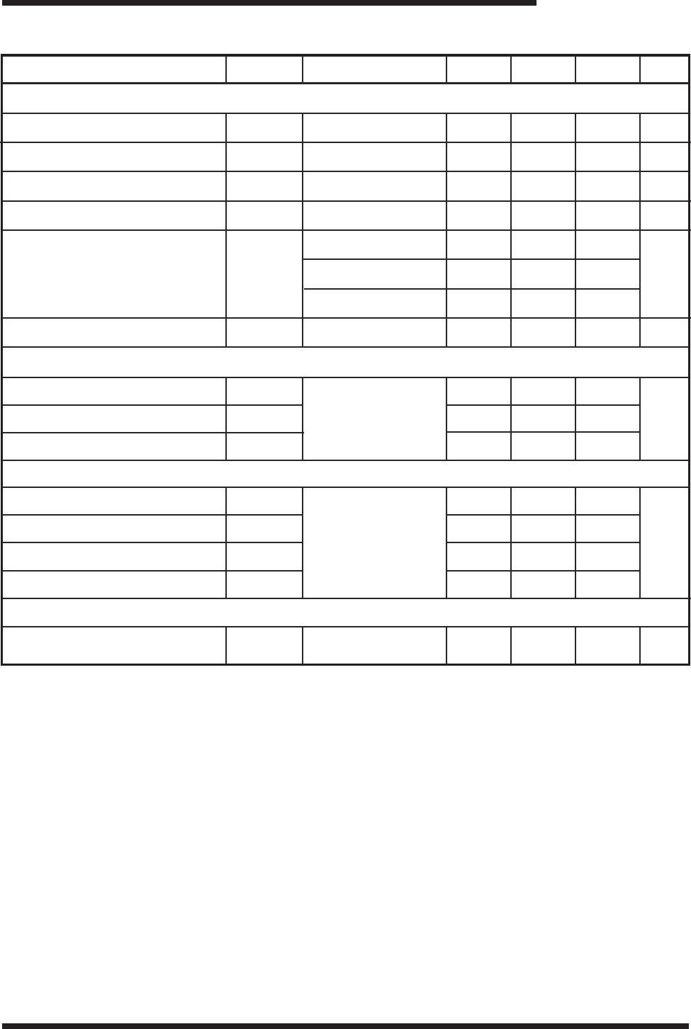
Drain-source breakdown voltage
VGS = 0V , ID = -250µA
Zero gate voltage drain current
Forward transconductance
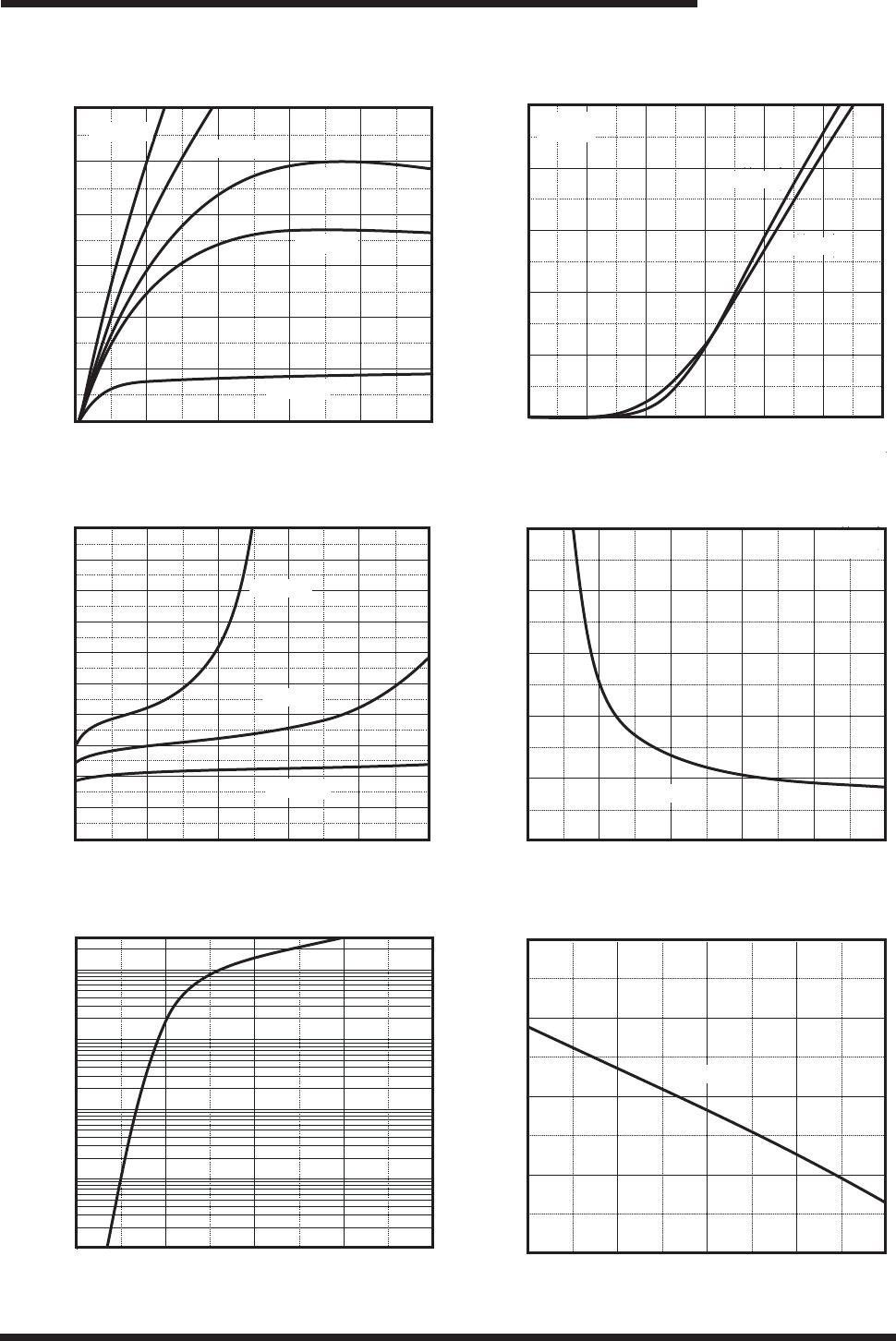
Reverse transfer capacitance
Input capacitance
Switching time (note4)
Turn-on delay time
Turn-off delay time
Rise time
Fall time
VDS = -20V , VGS = 0V
V = -1.8V , GS ID = -500mA
VDS = -10V , ID = -540mA
VDD = -10V, ID = -200mA
VGS = -4.5V , RG = 10Ω
V(BR) DSS
IDSS
gfs
Coss
Crss
td(on)
tr
td(off)
tf
-20
-1
0.8
9
5.8
32.7
20.3
V
S
pF
nS
ciss
170
Page 2
REV:A
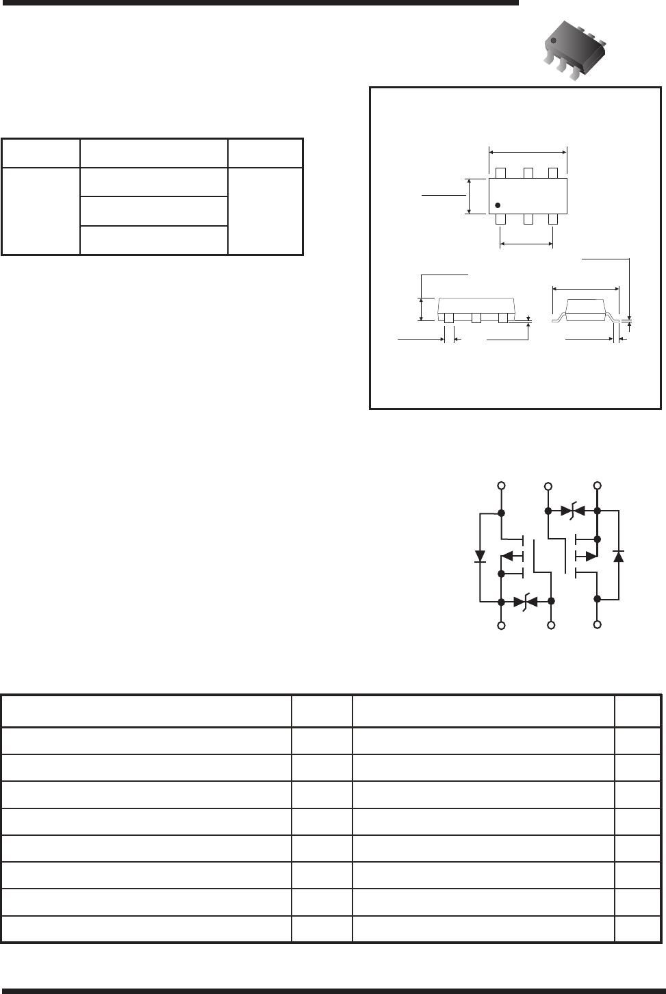
QW-BTR52
Comchip Technology CO., LTD.
MOSFET
Comchip
S M D D i o d e S p e c i a l i s t
Dynamic (note 4)characteristics
Output capacitance
25
15
On/Off States
Electrical Characteristics (at TA=25°C unless otherwise noted)
Company reserves the right to improve product design , functions and reliability without notice.
µA
VDS = -16V , VGS = 0V
f=1MHZ
VDS = VGS , ID = -250µA
-1.1
V
-0.35
Gate threshold voltage (note 3)
VGS(th)
Gate-body leakage current
VGS = ±10V, VDS = 0V
IGSS ±20
µA
RDS(on)
V = -4.5V , GS ID = -1A
520
V = -2.5V , GS ID = -800mA
950
mΩ
700
IS = -0.5A , VGS = 0V
VSD
-1.2
V
Drain-source on-state resistance (note 3)
Drain-source diode characteristics
Drain-source diode forward voltage
(note 3)
Parameter
Conditions
Symbol
Min
Typ
Max
Unit
Notes:
1. Repetitive rating: Pulse width limited by maximum junction temperture.
2. This test is performed with no heat sink at Ta=25°C.
3. Pulse test: Pulse width≤300µs, Duty cycle 0.5%.≤
4. These parameters have no way to verify.