ZL30111 Data Sheet
13
Zarlink Semiconductor Inc.
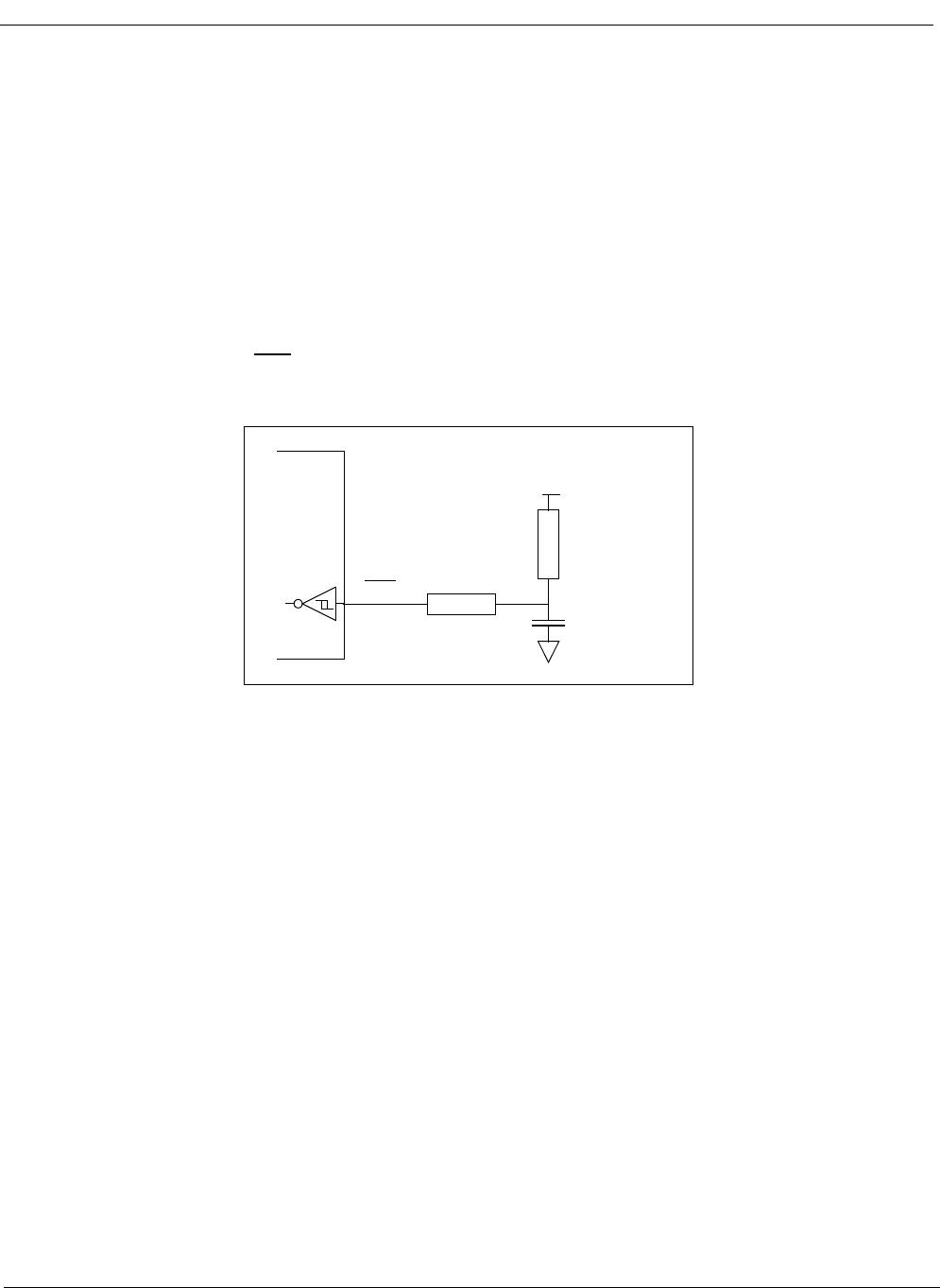
5.2.2 Crystal Oscillator
Alternatively, a Crystal Oscillator may be used. The accuracy of a crystal oscillator depends on the crystal tolerance
as well as the load capacitance tolerance. Typically, for a 20 MHz crystal specified with a 32 pF load capacitance,
each 1 pF change in load capacitance contributes approximately 9 ppm to the frequency deviation. Consequently,
capacitor tolerances and stray capacitances have a major effect on the accuracy of the oscillator frequency.
The crystal should be a fundamental mode type - not an overtone. The fundamental mode crystal permits a simpler
oscillator circuit with no additional filter components and is less likely to generate spurious responses. A typical
crystal oscillator specification is shown in Table 2.
.
1 Frequency 20 MHz
2 Tolerance as required (better than +/-50ppm)
3 Oscillation mode fundamental
4 Resonance mode parallel
5 Load capacitance as required
6 Maximum series resistance 50
Table 2 - Crystal Oscillator Specification
ZL30111 Data Sheet
14
Zarlink Semiconductor Inc.
5.3 Power Up Sequence
The ZL30111 requires that the 3.3 V supply is not powered up after the 1.8 V supply. This is to prevent the risk of
latch-up due to the presence of protection diodes in the IO pads.
Two options are given:
1. Power-up the 3.3 V supply fully first, then power up the 1.8 V supply
2. Power up the 3.3 V supply and the 1.8 V supply simultaneously, ensuring that the 3.3 V supply is never lower
than a few hundred millivolts below the 1.8 V supply (e.g., by using a schottky diode or controlled slew rate)
5.4 Reset Circuit
A simple power up reset circuit with about a 60 µs reset low time is shown in Figure 6. Resistor R
P
is for protection
only and limits current into the RST
pin during power down conditions. The reset low time is not critical but should
be greater than 300 ns.
Figure 6 - Power-Up Reset Circuit
+3.3 V
RST
R
P
1 k
C
10 nF
R
10 k
ZL30111
ZL30111 Data Sheet
15
Zarlink Semiconductor Inc.
6.0 Characteristics
6.1 AC and DC Electrical Characteristics
* Exceeding these values may cause permanent damage. Functional operation under these conditions is not implied.
* Voltages are with respect to ground (GND) unless otherwise stated.
Absolute Maximum Ratings*
Parameter Symbol Min. Max. Units
1 Supply voltage V
DD_R
-0.5 4.6 V
2 Core supply voltage V
CORE_R
-0.5 2.5 V
3 Voltage on any digital pin V
PIN
-0.5 6 V
4 Voltage on OSCi and OSCo pin V
OSC
-0.3 V
DD
+ 0.3 V
5 Current on any pin I
PIN
30 mA
6 Storage temperature T
ST
-55 125 °C
7 TQFP 64 pin package power dissipation P
PD
500 mW
8 ESD rating V
ESD
2 kV
Recommended Operating Conditions*
Characteristics Sym. Min. Typ. Max. Units
1 Supply voltage V
DD
3.1 3.30 3.5 V
2 Core supply voltage V
CORE
1.7 1.80 1.9
V
3 Operating temperature T
A
-40 25 85 °C
4 Input Voltage V
I
03.33.5 V

ZL30111QDG1

Mfr. #:
Manufacturer:
Microchip / Microsemi
Description:
Clock Generators & Support Products Pb Free POTS Line Card PLL
Lifecycle:
New from this manufacturer.
Delivery:
DHL FedEx Ups TNT EMS
Payment:
T/T Paypal Visa MoneyGram Western Union

Products related to this Datasheet