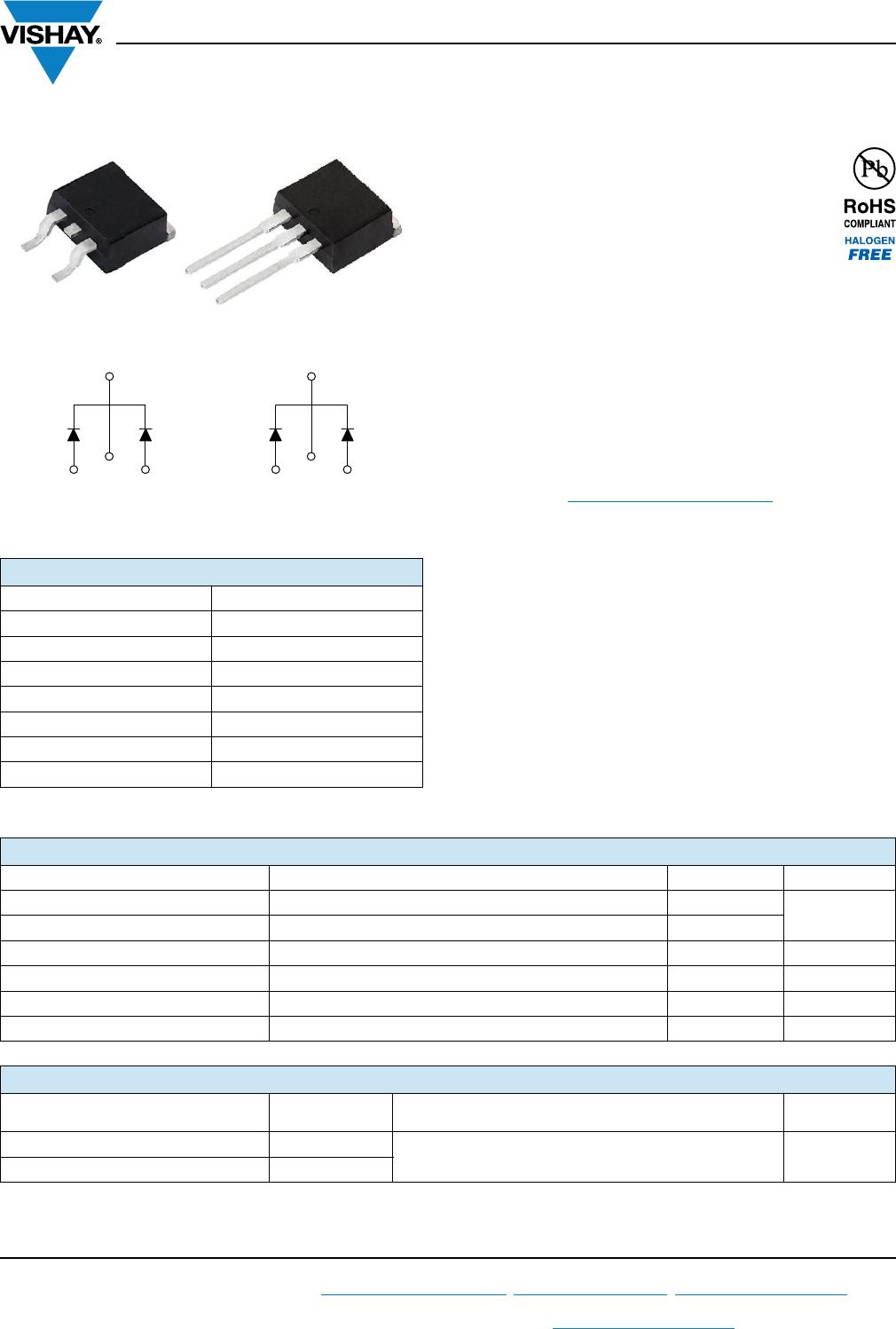
VS-MBRB4045CT-M3, VS-MBR4045CT-1-M3
www.vishay.com
Vishay Semiconductors
Revision: 06-Nov-17
2
Document Number: 96408
For technical questions within your region: DiodesAmericas@vishay.com
, DiodesAsia@vishay.com, DiodesEurope@vishay.com
THIS DOCUMENT IS SUBJECT TO CHANGE WITHOUT NOTICE. THE PRODUCTS DESCRIBED HEREIN AND THIS DOCUMENT
ARE SUBJECT TO SPECIFIC DISCLAIMERS, SET FORTH AT www.vishay.com/doc?91000
Note
(1)
Pulse width < 300 μs, duty cycle < 2 %
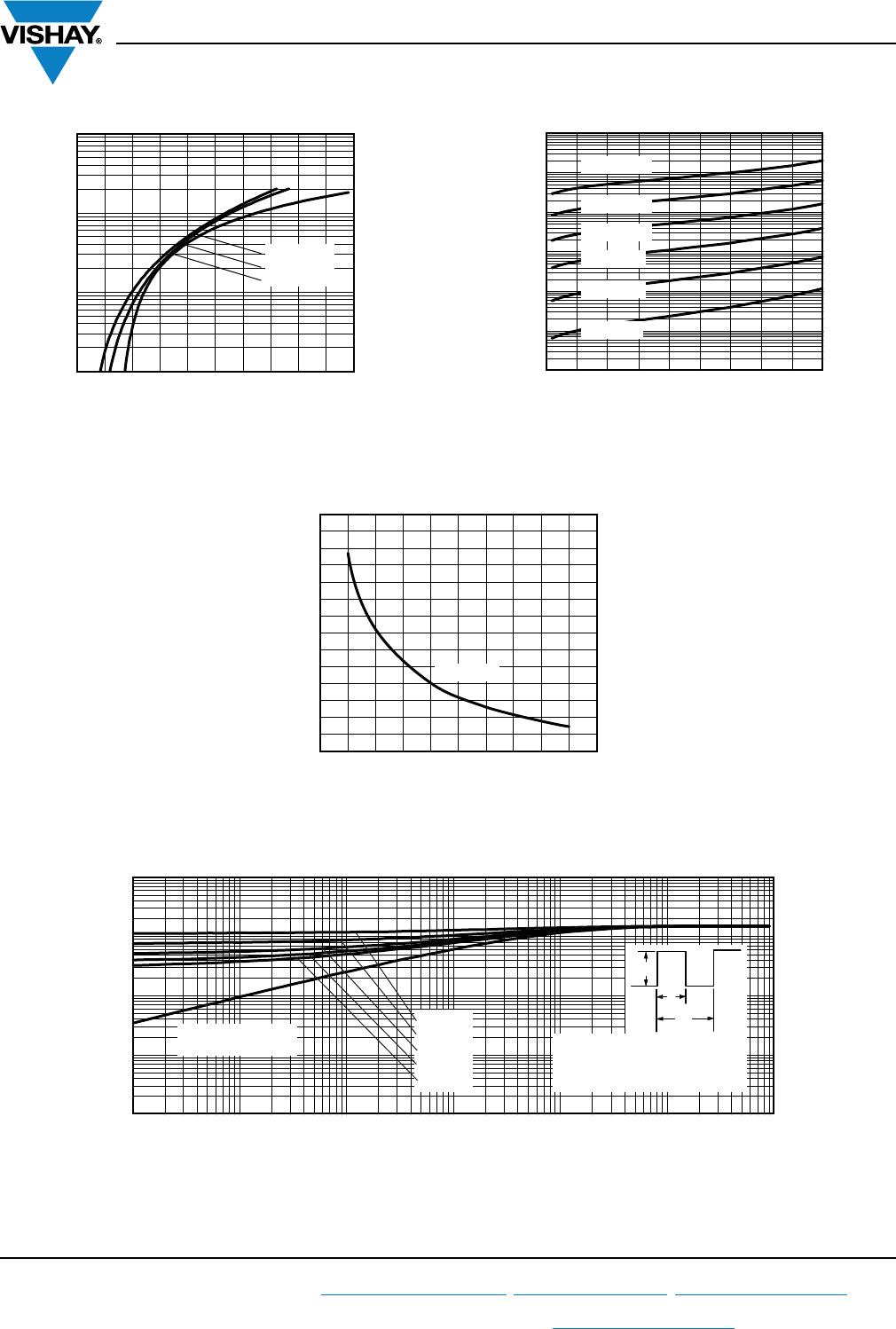
ABSOLUTE MAXIMUM RATINGS
PARAMETER SYMBOL TEST CONDITIONS VALUES UNITS
Maximum average
forward current
per leg
I
F(AV)
T
C
= 118 °C, rated V
R
20
A
per device 40
Peak repetitive forward current per leg I
FRM
Rated V
R
, square wave, 20 kHz, T
C
= 118 °C 40
Maximum peak one cycle non-repetitive
peak surge current per leg
I
FSM
5 μs sine or 3 μs rect. pulse
Following any rated
load condition and with
rated V
RRM
applied
900
10 ms sine or 6 ms rect. pulse 210
Non-repetitive avalanche energy per leg E
AS
T
J
= 25 °C, I
AS
= 3 A, L = 4.4 mH 20 mJ
Repetitive avalanche current per leg I
AR
Current decaying linearly to zero in 1 μs
Frequency limited by T
J
maximum V
A
= 1.5 x V
R
typical
3A
ELECTRICAL SPECIFICATIONS
PARAMETER SYMBOL TEST CONDITIONS VALUES UNITS
Maximum forward voltage drop V
FM
(1)
20 A
T
J
= 25 °C
0.60
V
40 A 0.78
20 A
T
J
= 125 °C
0.58
40 A 0.75
Maximum instantaneous
reverse current
I
RM
(1)
T
J
= 25 °C
Rated DC voltage
1
mAT
J
= 100 °C 50
T
J
= 125 °C 95
Maximum junction capacitance C
T
V
R
= 5 V
DC
(test signal range 100 kHz to 1 MHz), 25 °C 900 pF
Typical series inductance L
S
Measured from top of terminal to mounting plane 8.0 nH
Maximum voltage rate of change dV/dt Rated V
R
10 000 V/μs
THERMAL - MECHANICAL SPECIFICATIONS
PARAMETER SYMBOL TEST CONDITIONS VALUES UNITS
Maximum junction temperature range T
J
-65 to 150
°C
Maximum storage temperature range T
Stg
-65 to 175
Maximum thermal resistance,
junction to case per leg
R
thJC
DC operation 1.5
°C/W
Typical thermal resistance,
case to heatsink
R
thCS
Mounting surface, smooth, and greased
(Only for TO-220)
0.50
Maximum thermal resistance,
junction to ambient
R
thJA
DC operation
(For D
2
PAK and TO-262)
50
Approximate weight
2g
0.07 oz.
Mounting torque
minimum
Non-lubricated threads
6 (5)
kgf · cm
(lbf · in)
maximum 12 (10)
Marking device
Case style D
2
PAK (TO-263AB) MBRB4045CT
Case style TO-262 MBR4045CT-1