7
Regulatory Information
The ASSR-1510, ASSR-1511, ASSR-1520 and ASSR-1530 are approved by the following organizations:
UL
Approved under UL 1577, component recognition program up to V
ISO
= 3750 V
RMS
CSA
Approved under CSA Component Acceptance Notice #5.
Insulation and Safety Related Speci cations
Parameter Symbol ASSR-1510
ASSR-1511
ASSR-1520 ASSR-1530 Units Conditions
Minimum External
Air Gap (Clearance)
L(101) 4.9 7.1 4.9 mm Measured from input terminals to output
terminals, shortest distance through air.
Minimum External
Tracking (Creepage)
L(102) 4.9 7.4 4.8 mm Measured from input terminals to output
terminals, shortest distance path along body.
Minimum Internal
Plastic Gap
(Internal Clearance)
0.08 0.08 0.08 mm Through insulation distance conductor to
conductor, usually the straight line
distance thickness between the emitter and
detector.
Tracking Resistance
(Comparative
Tracking Index)
CTI 175 175 175 V DIN IEC 112/VDE 0303 Part 1
Isolation Group
(DIN VDE0109)
IIIa IIIa IIIa Material Group (DIN VDE 0109)
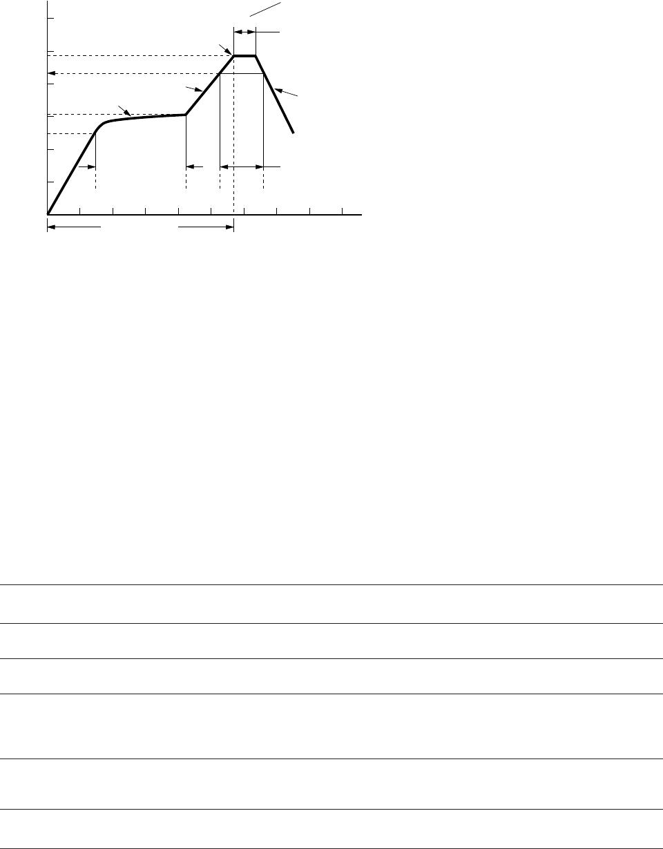
Lead Free IR Pro le
217°C
RAMP-DOWN
6
°C/SEC. MAX.
RAMP-UP
3
°C/SEC. MAX.
150 - 200°C
260 +0/-5
°C
t 25
°C to PEAK
60 to 150 SEC.
20-40 SEC.
TIME WITHIN 5
°C of ACTUAL
PEAK TEMPERATURE
t
p
t
s
PREHEAT
60 to 180 SEC.
t
L
T
L
T
smax
T
smin
25
T
p
TIME (SECONDS)
TEMPERATURE (°C)
NOTES:
THE TIME FROM 25°C to PEAK TEMPERATURE = 8 MINUTES MAX.
T
smax
= 200°C, T
smin
= 150°C
Use of non-chlorine-activated fluxes is highly recommended.
8
Absolute Maximum Ratings
Parameter Symbol Min. Max. Units Note
Storage Temperature T
S
-55 125
C
Operating Temperature T
A
-40 85
C
Junction Temperature T
J
125
C
Lead Soldering Cycle Temperature 260
C
Time 10 s
Input Current Average I
F
25 mA
Surge 50
Transient 1000
Reversed Input Voltage V
R
5V
Input Power Dissipation ASSR-1510 P
IN
40 mW
ASSR-1511 P
IN
40 mW
ASSR-1520
ASSR-1530
P
IN
80 mW
Output Power Dissipation ASSR-1510 P
O
500 mW
ASSR-1511 P
O
800 mW
ASSR-1520
ASSR-1530
P
O
700 mW
Average Output Current
(T
A
= 25°C, T
C
100°C)
I
O
1.0 A 1
ASSR-1511
Connection B
I
O
2.0 A
Output Voltage (T
A
= 25°C) V
O
-60 60 V 2
ASSR-1511
Connection B
V
O
060V2
Solder Re ow Temperature Pro le See Lead Free IR Pro le
Recommended Operating Conditions
Parameter Symbol Min. Max. Units Note
Input Current (ON) I
F(ON)
320mA3
Input Voltage (OFF) V
F(OFF)
0 0.8 V
Operating Temperature T
A
-40 +85
C
Package Characteristics
Unless otherwise speci ed, T
A
= 25°C.
Parameter Sym. Min. Typ. Max. Units Conditions Note
Input-Output Momentary
Withstand Voltage
V
ISO
3750 Vrms
RH
50%,
t = 1 min
4, 5
Input-Output Resistance R
I-O
10
12
V
I-O
= 500 Vdc
Input-Output Capacitance
ASSR-1510 C
I-O
0.4 pF f = 1 MHz; V
I-O
= 0 Vdc 4
ASSR-1511 C
I-O
0.5 pF f = 1 MHz; V
I-O
= 0 Vdc
ASSR-1520
ASSR-1530
C
I-O
0.8 pF f = 1 MHz; V
I-O
= 0 Vdc
9
Electrical Speci cations (DC)
Over recommended operating T
A
= -40°C to 85°C, I
F
= 5mA to 10mA, unless otherwise speci ed.
Parameter Sym. Min. Typ. Max. Units Conditions Fig. Note
Output Withstand
Voltage
|V
O(OFF)
|6065 V
V
F
=0.8V, I
O
=250 A, T
A
=25C
55 V
V
F
=0.8V, I
O
=250 A
5
Output Leakage
Current
I
O(OFF)
0.5 100 nA
V
F
=0.8V, V
O
=60V, T
A
=25C
1
A
V
F
=0.8V, V
O
=60V 6
Output O set
Voltage
|V
(OS)
|1
V
I
F
=5mA, I
O
=0mA
Input Reverse
Breakdown Volt-
age
V
R
5V
I
R
=10 A
Input Forward
Voltage
V
F
1.1 1.3 1.65 V I
F
=5mA 8, 9
Output
On-resistance
R
(ON)
0.35 0.5
I
F
=5mA, I
O
=1A,
Pulse
30ms, T
A
=25C
10, 11 6
ASSR-1511
Connection B
R
(ON)
0.12 0.2
I
F
=5mA, I
O
=2A,
Pulse
30ms, T
A
=25C
Switching Speci cations (AC)
Over recommended operating T
A
= -40°C to 85°C, I
F
= 5mA to 10mA, unless otherwise speci ed.
Parameter Sym. Min. Typ. Max. Units Conditions Fig. Note
Turn On Time T
ON
0.5 1.0 ms
I
F
=5mA, I
O
=1A, T
A
=25C
12, 16
2.0 ms I
F
=5mA, I
O
=1A 13
0.25 0.5 ms
I
F
=10mA, I
O
=1A, T
A
=25C
1.0 ms I
F
=10mA, I
O
=1A
Turn O Time T
OFF
0.03 0.2 ms
I
F
=5mA, I
O
=1A, T
A
=25C
14, 16
0.5 ms I
F
=5mA, I
O
=1A 15
0.02 0.15 ms
I
F
=10mA, I
O
=1A, T
A
=25C
0.2 ms I
F
=10mA, I
O
=1A
Output Transient
Rejection
dV
O
/dt 1 7
kV/s V
O
=60V, T
A
=25C
17
Input-Output
Transient Rejection
dV
I-O
/dt 1
10 kV/s V
I-O
=1000V, T
A
=25C
18
Notes:
1. For derating, refer to Figure 1, 2, 3 and 4.
2. The voltage across the output terminals of the relay should not exceed this rated withstand voltage. Over-voltage protection circuits should
be added in some applications to protect against over-voltage transients.
3. Threshold to switch device is I
F
0.5mA, however, for quali ed device performance over temperature range, it is recommended to operate at
I
F
=5mA.
4. Device is considered as a two terminal device:
ASSR-1510 - pin 1, 2 shorted and pin 3, 4 shorted.
ASSR-1511 - pin 1, 2, 3 shorted and pin 4, 5, 6 shorted.
ASSR-1520 and ASSR-1530 - pin 1, 2, 3, 4 shorted and pin 5, 6, 7, 8 shorted.
5. The Input-Output Momentary Withstand Voltage is a dielectric voltage rating that should not be interpreted as an input-output continuous
voltage rating. For the continuous voltage rating refer to the IEC/EN/DIN EN 60747-5-2 Insulation Characteristics Table (if applicable), your
equipment level safety speci cation, or Avago Technologies Application Note 1074, Optocoupler Input-Output Endurance Voltage.
6. During the pulsed R
(ON)
measurement ( I
O
duration 30ms), ambient (T
A
) and case temperature (T
C
) are equal.

ASSR-1530-005E

Mfr. #:
Manufacturer:
Broadcom / Avago
Description:
Solid State Relays - PCB Mount SSR Photo MOSFET (60V 1.0A)
Lifecycle:
New from this manufacturer.
Delivery:
DHL FedEx Ups TNT EMS
Payment:
T/T Paypal Visa MoneyGram Western Union