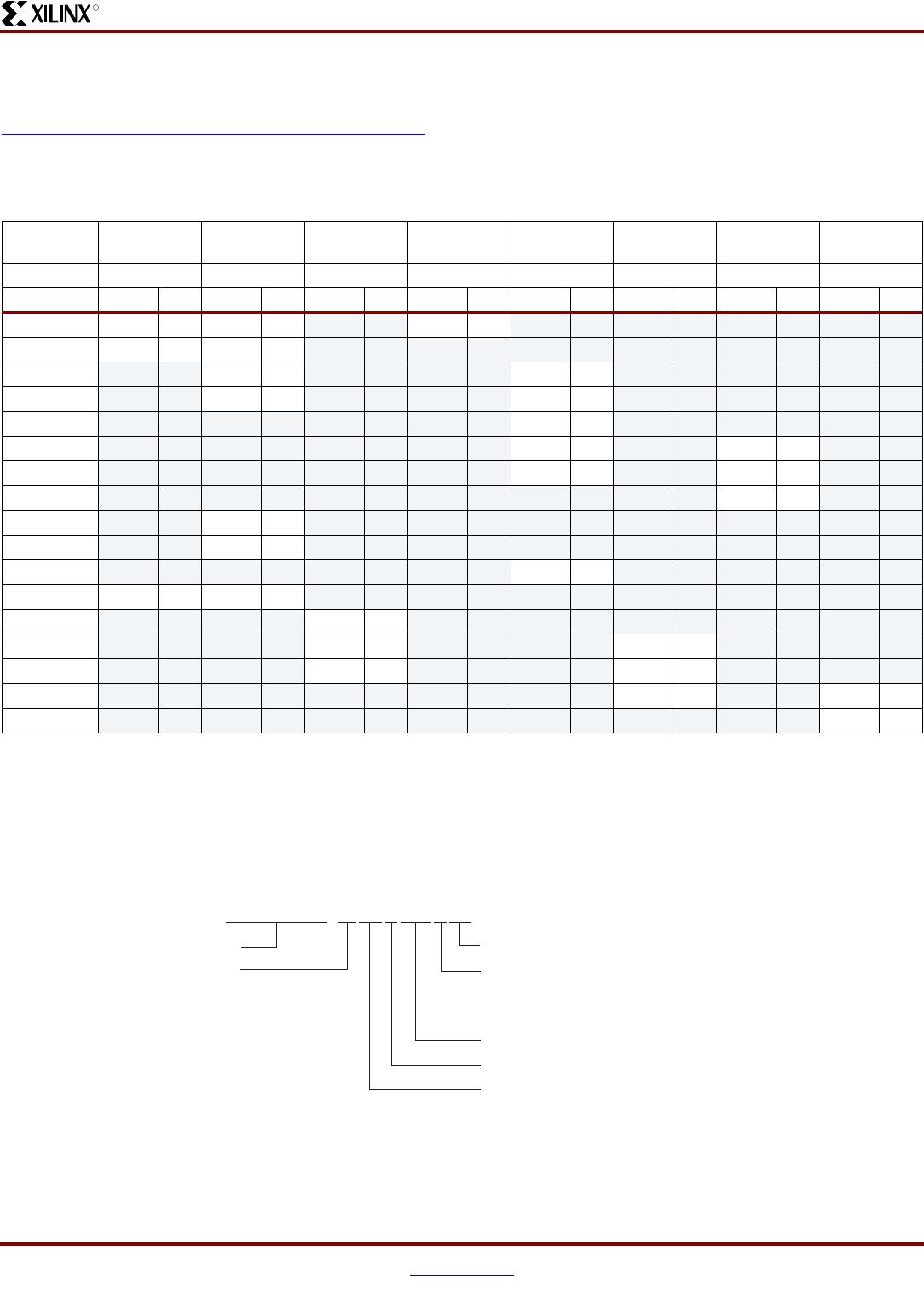
Virtex-4 Family Overview
DS112 (v3.1) August 30, 2010 www.xilinx.com
Product Specification 8
R
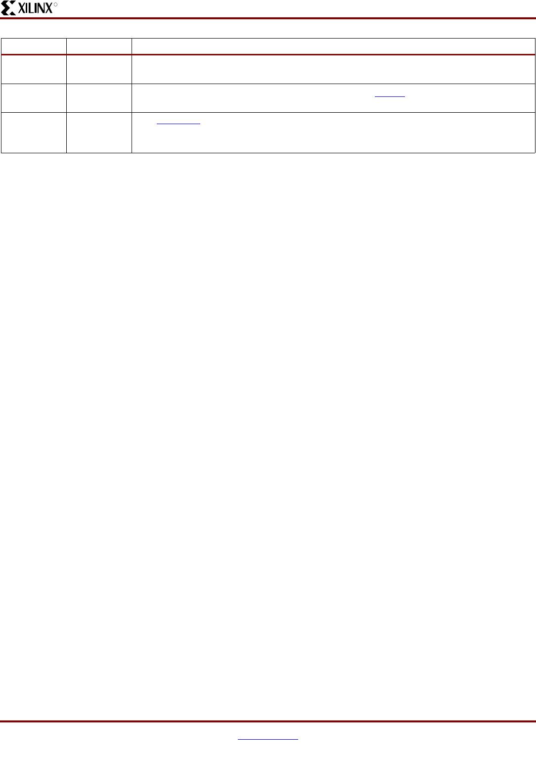
Virtex-4 Documentation
Complete and up-to-date documentation of the Virtex-4
family of FPGAs is available on the Xilinx web site. In addi-
tion to the most recent Virtex-4 Family Overview, the follow-
ing files are also available for download:
Virtex-4 FPGA Data Sheet: DC and Switching
Characteristics
This data sheet contains the DC and Switching Characteris-
tic specifications for the Virtex-4 family.
Virtex-4 FPGA User Guide
This guide includes chapters on:
• Clocking Resources
• Digital Clock Manager (DCM)
• Phase-Matched Clock Dividers (PMCD)
• Block RAM and FIFO memory
• Configurable Logic Blocks (CLBs)
• SelectIO Resources
• SelectIO Logic Resources
• Advanced SelectIO Logic Resources
XtremeDSP for Virtex-4 FPGAs User Guide
This guide describes the DSP48 slice and includes refer-
ence designs for using DSP48 math functions and various
FIR filters.
Virtex-4 FPGA Configuration Guide
This all-encompassing configuration guide includes chap-
ters on configuration interfaces (serial and SelectMAP), bit-
stream encryption, Boundary-Scan and JTAG configuration,
and reconfiguration techniques.
Virtex-4 FPGA Packaging and Pinout Specification
This specification includes the tables for device/package
combinations and maximum I/Os, pin definitions, pinout
tables, pinout diagrams, mechanical drawings, and thermal
specifications.
Virtex-4 FPGA PCB Designer’s Guide
This guide describes PCB guidelines for the Virtex-4 family.
It covers SelectIO signaling, RocketIO signaling, power dis-
tribution systems, PCB breakout, and parts placement.
Virtex-4 RocketIO Multi-Gigabit Transceiver User Guide
This guide describes the RocketIO Multi-Gigabit Transceiv-
ers available in the Virtex-4 FX family.
Virtex-4 FPGA Embedded Tri-Mode Ethernet MAC User
Guide
This guide describes the Embedded Tri-Mode Ethernet
Media Access Controller available in the Virtex-4 FX family.
PowerPC 405 Processor Block Reference Guide
This guide is updated to include the PowerPC 405 proces-
sor block available in the Virtex-4 FX family.
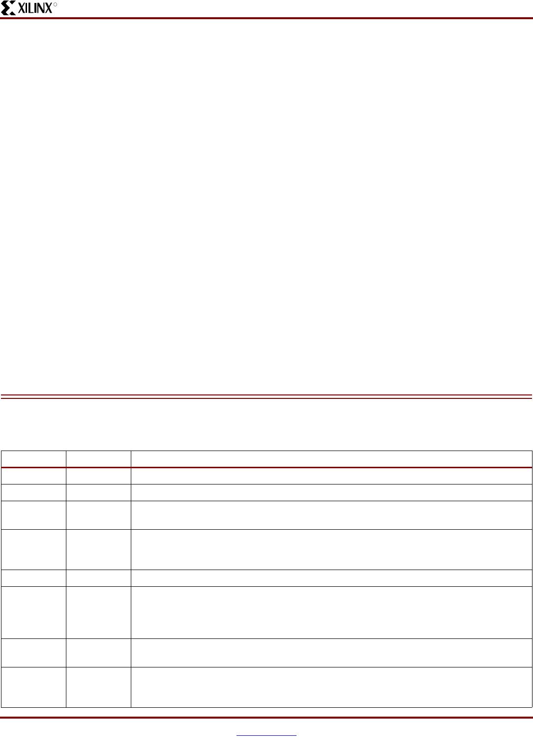
Revision History
The following table shows the revision history for this document.
Date Version Revision
08/02/04 1.0 Initial Xilinx release. Printed Handbook version.
09/10/04 1.1 Typographical edits.
12/08/04 1.2 • Removed System Monitor and ADC references.
• Edited Ethernet MAC section.
03/26/05 1.3 • Removed legacy CLB reference and typographical edits.
• Edited serial transceiver sections.
•In Table 2 added FFG Pb-Free packages.
06/17/05 1.4 Added note to Ta bl e 2 for SparseChevron pinouts.
02/10/06 1.5 • Removed FCRAM-II support.
• Added note 3 to Ta bl e 1 .
• Revised the CLB numbers for XC4VFX40 devices in Table 1 .
• Added stepping to order information example in Figure 1.
10/10/06 1.6 • Changed maximum transceiver rate to 6.5 Gb/s.
• Removed FF1760 package from Ta ble 2 .
01/23/07 2.0 Revision number jumped to 2.0 to correlate to data sheet (DS302) major revision.
• Table 1 : Corrected typo: XC4VFX40 number of slices = 18,624.
• Table 2 : Added column for FF676 package. Rewrote table footnotes.