LT1884CS8#PBF

LT1884/LT1885
4
The denotes the specifications which apply over the full operating temperature range, otherwise specifications are at T
A
= 25°C.
Single supply operation V
EE
= 0, V
CC
= 5V; V
CM
= V
CC
/2 unless otherwise noted. (Note 5)
SYMBOL PARAMETER CONDITIONS MIN TYP MAX UNITS
V
OS
Offset Voltage Match (LT1884A) 30 70 µV
0°C < T
A
< 70°C 125 µV
–40°C < T
A
< 85°C 160 µV
Offset Voltage Match (LT1884/LT1885) (Note 7) 35 125 µV
0°C < T
A
< 70°C 195 µV
–40°C < T
A
< 85°C 235 µV
Offset Voltage Match Drift (Notes 6, 7) 0.4 1.2 µV/°C
I
B
+ Noninverting Bias Current Match 200 600 pA
(LT1884A) 0°C < T
A
< 70°C 700 pA
–40°C < T
A
< 85°C 850 pA
Noninverting Bias Current Match (Notes 7, 9) 250 1200 pA
(LT1884/LT1885) 0°C < T
A
< 70°C 1600 pA
–40°C < T
A
< 85°C 1900 pA
CMRR Common Mode Rejection Match (Notes 7, 9) 104 125 dB
PSRR Positive Power Supply Rejection Match V
EE
= 0, V
CM
= 1.5V
(Notes 7, 9) 0°C < T
A
< 85°C, 2.7V < V
CC
< 32V 104 126 dB
T
A
= –40°C, 3V < V
CC
< 32V 104 126 dB
ELECTRICAL CHARACTERISTICS
The denotes the specifications which apply over the full operating temperature range, otherwise specifications are at T
A
= 25°C.
Split supply operation V
S
= ±15V; V
CM
= 0V unless otherwise noted. (Note 5)
SYMBOL PARAMETER CONDITIONS MIN TYP MAX UNITS
V
OS
Input Offset Voltage (LT1884A) 25 50 µV
0°C < T
A
< 70°C 85 µV
–40°C < T
A
< 85°C 110 µV
Input Offset Voltage (LT1884/LT1885) 30 80 µV
0°C < T
A
< 70°C 125 µV
–40°C < T
A
< 85°C 150 µV
Input Offset Voltage Drift (Note 6) 0°C < T
A
< 70°C 0.3 0.8 µV/°C
–40°C < T
A
< 85°C 0.3 0.8 µV/°C
I
OS
Input Offset Current (LT1884A) 150 300 pA
0°C < T
A
< 70°C 400 pA
–40°C < T
A
< 85°C 500 pA
Input Offset Current (LT1884/LT1885) 150 900 pA
0°C < T
A
< 70°C 1200 pA
–40°C < T
A
< 85°C 1400 pA
I
B
Input Bias Current (LT1884A) 150 400 pA
0°C < T
A
< 70°C 500 pA
–40°C < T
A
< 85°C 600 pA
Input Bias Current (LT1884/LT1885) 150 900 pA
0°C < T
A
< 70°C 1200 pA
–40°C < T
A
< 85°C 1400 pA
Input Noise Voltage 0.1Hz to 10Hz 0.4 µV
P-P
e
n
Input Noise Voltage Density f = 1kHz 9.5 nV/Hz
i
n
Input Noise Current Density f = 1kHz 0.05 pA/Hz
V
CM
Input Voltage Range V
EE
+ 1.0 V
CC
– 1.0 V
V
EE
+ 1.2 V
CC
– 1.2 V
CMRR Common Mode Rejection Ratio 13.5V < V
CM
< 13.5V 114 130 dB
LT1884/LT1885
5
SYMBOL PARAMETER CONDITIONS MIN TYP MAX UNITS
+PSRR Positive Power Supply Rejection Ratio V
EE
= –15V, V
CM
= 0V; 1.5V < V
CC
< 18V 114 132 dB
PSRR Negative Power Supply Rejection Ratio V
CC
= 15V, V
CM
= 0V; –1.5V < V
EE
< –18V 106 132 dB
Minimum Operating Supply Voltage ±1.2 ±1.35 V
A
VOL
Large-Signal Voltage Gain R
L
= 10k; –13.5V < V
OUT
< 13.5V 1000 1600 V/mV
700 V/mV
R
L
= 2k; –13.5V < V
OUT
< 13.5V 250 420 V/mV
175 V/mV
R
L
= 1k; –12V < V
OUT
< 12V 100 230 V/mV
75 V/mV
V
OL
Output Voltage Swing Low No Load 20 40 mV
(Referred to V
EE
)I
SINK
= 100µA 25 50 mV
I
SINK
= 1mA 70 150 mV
I
SINK
= 5mA 270 600 mV
V
OH
Output Voltage Swing High No Load 160 220 mV
(Referred to V
CC
)I
SOURCE
= 100µA 160 230 mV
I
SOURCE
= 1mA 180 300 mV
I
SOURCE
= 5mA 360 600 mV
I
S
Supply Current Per Amplifier V
S
= ±15V 0.85 1.1 mA
1.6 mA
I
SC
Short-Circuit Current V
OUT
Short to V
EE
15 50 mA
V
OUT
Short to V
CC
15 30 mA
GBW Gain-Bandwidth Product f = 20kHz 1.5 2.2 MHz
t
S
Settling Time 0.01%, V
OUT
= – 5V to 5V, 17 µs
A
V
= –1, R
L
= 2k
SR
+
Positive Slew Rate A
V
= –1 0.5 1.0 V/µs
0.4 V/µs
SR
Negative Slew Rate A
V
= –1 0.40 0.7 V/µs
0.26 V/µs
V
OS
Offset Voltage Match (LT1884A) (Note 7) 35 70 µV
0°C < T
A
< 70°C 125 µV
–40°C < T
A
< 85°C 160 µV
Offset Voltage Match (LT1884/LT1885) (Note 7) 35 125 µV
0°C < T
A
< 70°C 175 µV
–40°C < T
A
< 85°C 235 µV
Offset Voltage Match Drift (Note 6, 7) 0.4 1.1 µV/°C
I
B
+
Noninverting Bias Current Match (Notes 7, 8) 200 600 pA
(LT1884A) 0°C < T
A
< 70°C 700 pA
–40°C < T
A
< 85°C 850 pA
Noninverting Bias Current Match (Notes 7, 8) 240 1200 pA
(LT1884/LT1885) 0°C < T
A
< 70°C 1600 pA
–40°C < T
A
< 85°C 1900 pA
CMRR Common Mode Rejection Match (Notes 7, 9) 106 125 dB
+PSRR Positive Power Supply Rejection Match V
EE
= –15V, V
CM
= 0V, 1.5V < V
CC
< 18V, 108 124 dB
(Notes 7, 9)
PSRR Negative Power Supply Rejection Match V
CC
= 15V, V
CM
= 0V, –1.5V < V
EE
< –18V, 102 132 dB
(Notes 7, 9)
The denotes the specifications which apply over the full operating temperature range, otherwise specifications are at T
A
= 25°C.
Split supply operation V
S
= ±15V; V
CM
= 0V unless otherwise noted. (Note 5)
ELECTRICAL CHARACTERISTICS
LT1884/LT1885
6
Note 1: Absolute Maximum Ratings are those values beyond which the life
of the device may be impaired.
Note 2: The inputs are protected by back-to-back diodes. If the differential
input voltage exceeds 0.7V, the input current should be limited to less than
10mA.
Note 3: A heat sink may be required to keep the junction temperature
below absolute maximum.
Note 4: The LT1884C/LT1885C and LT1884I/LT1885I are guaranteed
functional over the operating temperature range of – 40°C to 85°C.
Note 5: The LT1884C/LT1885C are designed, characterized and expected
to meet specified performance from –40°C to 85°C but are not tested or
QA sampled at these temperatures. LT1884I is guaranteed to meet
specified performance from – 40°C to 85°C.
Note 6: This parameter is not 100% tested.
Note 7: Matching parameters are the difference between amplifiers A and
B in the LT1884 and between amplifiers A and D and B and C in the
LT1885.
Note 8: This parameter is the difference between the two noninverting
input bias currents.
Note 9: CMRR and PSRR are defined as follows: CMRR and PSRR are
measured in µV/V on each amplifier. The difference is calculated in µV/V
and then converted to dB.
ELECTRICAL CHARACTERISTICS
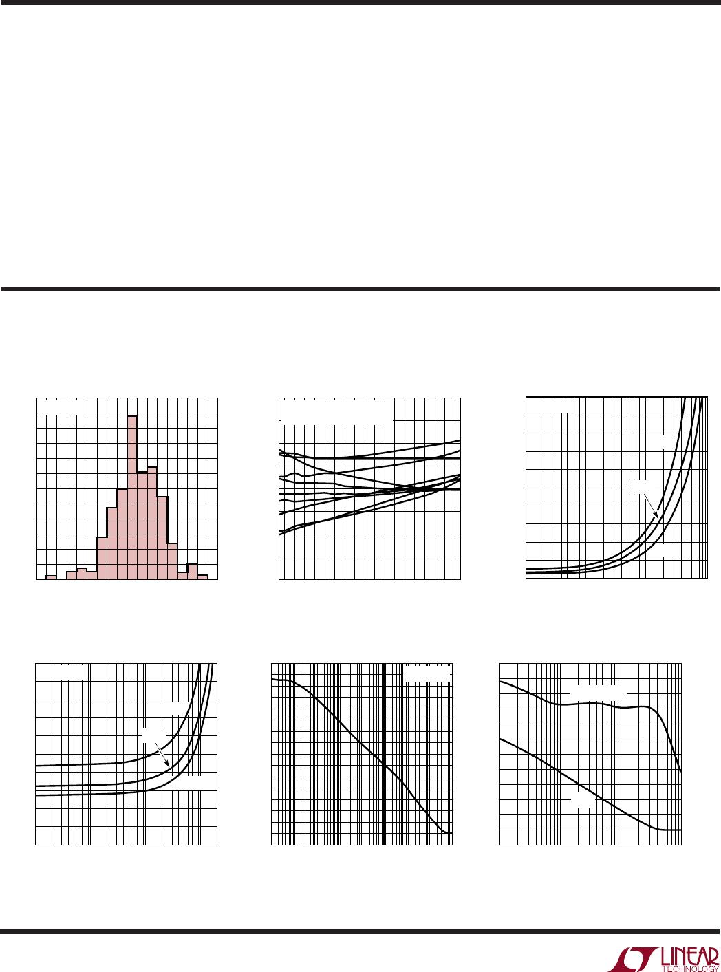
Distribution of Offset Voltage Drift
TYPICAL PERFOR A CE CHARACTERISTICS
UW
OFFSET VOLTAGE DRIFT (µV/°C)
0.9 –0.7 0.5 –0.3 0.1 0.1 0.3 0.5 0.7 0.9
PERCENT OF UNITS (%)
12
16
20
24
18845 G01
8
4
0
V
S
= ±15V
TEMPERATURE (°C)
–50 –30 –10 10 30 50 70 90 110125
INPUT OFFSET VOLTAGE (µV)
50
100
150
200
18845 G02
0
–50
100
150
200
TEMPCO: –55°C TO 125°C
10 REPRESENTATIVE UNITS
I
SINK
(V
OUT
– V
EE
) (mV)
500
400
300
200
100
0
10µA 1mA 10mA
18845 G03
100µA
125°C
–55°C
25°C
V
S
= ±15V
Input Offset Voltage
vs Temperature
V
OUT
vs I
SOURCE
V
OUT
vs I
SINK
I
SOURCE
(V
CC
– V
OUT
) (mV)
500
400
300
200
100
0
10µA 1mA 10mA
18845 G04
100µA
125°C
V
S
= ±15V
–55°C
25°C
Gain vs Frequency
FREQUENCY (Hz)
GAIN (dB)
140
120
100
80
60
40
20
0
–20
18845 G05
0.1 1 10 100 1k 10k 100k 1M 10M
V
S
= ±15V
Gain, Phase Shift vs Frequency
FREQUENCY (Hz)
VOLTAGE GAIN (dB)
100
90
80
70
60
50
40
30
20
10
0
–10
–20
PHASE SHIFT (DEG)
–80
–90
100
110
120
130
140
150
160
170
180
18845 G06
10k 100k 1M 10M
PHASE SHIFT
GAIN

LT1884CS8#PBF

Mfr. #:
Manufacturer:
Analog Devices Inc.
Description:
Precision Amplifiers Dual R-to-R Output Picoamp OA
Lifecycle:
New from this manufacturer.
Delivery:
DHL FedEx Ups TNT EMS
Payment:
T/T Paypal Visa MoneyGram Western Union