[4]
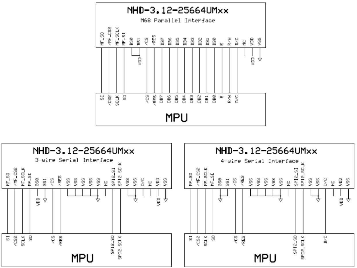
3. InterfaceDescription
3.1. ParallelInterface:
PinNo. Symbol External
Connection
FunctionDescription
1 VSS PowerSupply Ground
2 VDD PowerSupply SupplyVoltageforOLEDandlogic.
3 NC‐NoConnect
4 D/C MPU Registerselectsignal.D/C=0:Command,D/C=1:Data
5 R/Wor/WR MPU 6800‐interface:
Read/Writeselectsignal,R/W=1:ReadR/W:=0:Write
8080‐interface:
ActiveLOWWritesignal.
6 Eor/RD MPU 6800‐interface:
Operationenablesignal.Fallingedgetriggered.
8080‐interface:
ActiveLOWReadsignal.
7‐14 DB0
DB7 MPU 8‐bitBi‐directionaldatabuslines.
15 /RES MPU ActiveLOWResetsignal.
16 /CS MPU ActiveLOWChipEnable signal.
17 BS1 MPU MPUInterfaceSelectsignal.
18 BS0 MPU MPUInterfaceSelectsignal.
19 MF_SCLK MPU Multi‐fontICSerialClockInput
20 MF_SI MPU Multi‐fontICSerialDataInput
21 /MF_CS2 MPU Multi‐fontICActiveLOWChipEnablesignal.
22 MF_SO MPU Multi‐fontICSerialDataOutput
3.2. SerialInterface:
PinNo. Symbol External
Connection
FunctionDescription
1 VSS PowerSupply Ground
2 VDD PowerSupply SupplyVoltageforOLEDandlogic.
3 NC‐NoConnect
4 D/C MPU Registerselectsignal.D/C=0:Command,D/C=1:Data
5‐6 VSS PowerSupply Ground
7 SCLK MPU SerialClocksignal.
8 SDIN MPU SerialDataInputsignal.
9 NC‐NoConnect
10‐14 VSS PowerSupply Ground
15 /RES MPU ActiveLOWResetsignal.
16 /CS MPU ActiveLOWChipEnablesignal.
17 BS1 MPU MPUInterfaceSelectsignal.
18 BS0 MPU MPUInterfaceSelectsignal.
19 MF_SCLK MPU Multi‐fontICSerialClockInput
20 MF_SI MPU Multi‐fontICSerialDataInput
21 /MF_CS2 MPU Multi‐fontICActiveLOWChipEnablesignal.
22 MF_SO MPU Multi‐fontICSerialDataOutput