SP3495E-3497E
4
HIGH SPEED +3.3V RS-485/RS-422 TRANSCEIVERS WITH +/-15KV ESD PROTECTION AND ADVANCED FAILSAFE REV. 1.0.0
CAUTION:
ESD (Electrostatic Discharge) sensitive device. Permanent damage may occur on unconnected devices subject to high energy electrostatic fields. Unused
devices must be stored in conductive foam or shunts. Personnel should be properly grounded prior to handling this device. The protective foam should be
discharged to the destination socket before devices are removed.
ABSOLUTE MAXIMUM RATINGS
These are stress ratings only and functional operation of the device at these ratings or any other above those indicated in the operation sections to the
specifications below is not implied. Exposure to absolute maximum rating conditions for extended periods of time may affect reliability and cause permanent
damage to the device.
V
CC
+6.0V
Input Voltage at control pins (RE
, DE and DI) -0.5V to (V
CC
+ 0.3V)
Voltage Range on A and B pins -9V to +14V
Storage Temperature Range -65°C to + 150°C
Power Dissipation
Maximum Junction Temperature 150°C
8-Pin SO θ
JA
= 128.4°C/W
14-Pin SO θ
JA
= 86°C/W
ELECTRICAL CHARACTERISTICS
UNLESS OTHERWISE NOTED: VCC = +3.0V TO +3.6V WITH T
A
FROM -40
O
C TO +85
O
C. TYPICAL VALUES ARE AT
V
CC = +3.3V AND 25
O
C.
SYMBOL PARAMETERS MIN.TYP.MAX.UNITS CONDITIONS
DRIVER DC CHARACTERISTICS
V
OD
Differential Driver Output Vcc V No Load
2.0 R
L
= 100(RS-422), Figure 3
1.5 R
L
= 54(RS-485), Figure 3
1.5 V
CM
= -7V, Figure 4
1.5 V
CM
= +12V, Figure 4
V
OD
Change in Magnitude of Differential
Output
-0.20 0.20 V R
L
= 100(RS-422), Figure 3,
See note 1
-0.20 0.20 R
L
= 54(RS-485), Figure 3,
See note 1
-0.20 0.20 V
CM
= -7V, Figure 4, See
note 1
-0.20 0.20 V
CM
= +12V, Figure 4, See note
1
V
OC
Driver Common Mode Output
Voltage steady state
1.3 2.5 V Figure 3
V
OC
Change in Magnitude of Common
Mode Output Voltage
-0.2 0.2 V Figure 3, See note 1
I
DSC
Driver Short Circuit Current Limit -250 mA V
OUT
Forced to -7V, Figure 5
250 mA V
OUT
Forced to +12V, Figure 5
SP3495E-3497E
5
REV. 1.0.0 HIGH SPEED +3.3V RS-485/RS-422 TRANSCEIVERS WITH +/-15KV ESD PROTECTION AND ADVANCED FAILSAFE
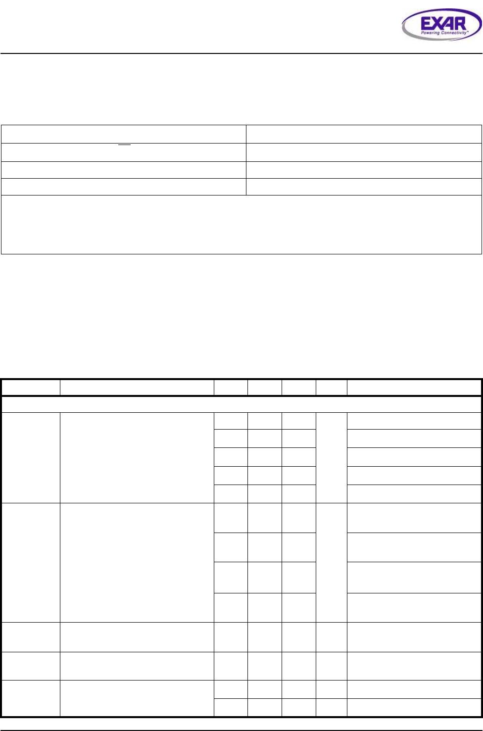
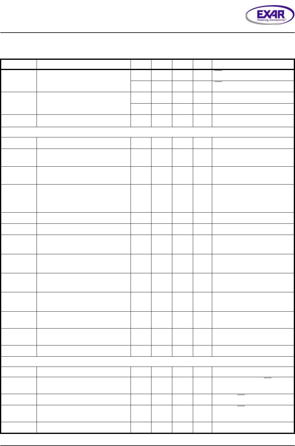
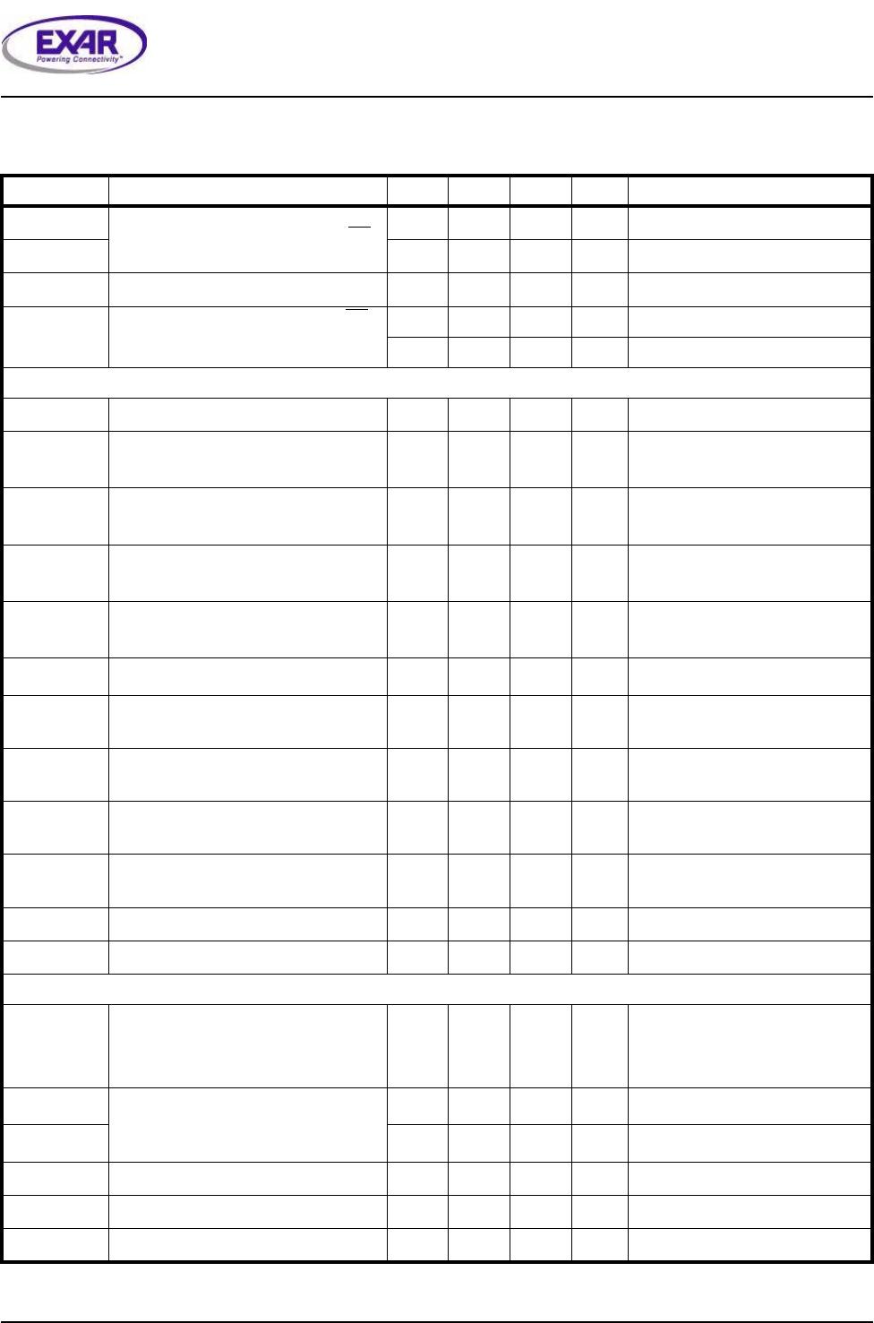
V
IH
Logic Input Thresholds (DI, DE, RE)
2.0 V Logic Input High
V
IL
0.8 V Logic Input Low
V
HYS
Driver Input Hysteresis 100 mV T
A
= 25°C
I
IN
Logic Input Current (DI, DE and RE)10uAIN = 0V
-10 uA IN = Vcc
Driver AC Characteristics
freq Data Signaling Rate 32 Mbps 1/t
UI
, Duty Cycle 40 to 60%
t
PLH
Driver Propagation Delay (low to
High)
51124nsC
L
= 50pF, R
L
= 54Ω,
freq = 8MHz, Figures 6 and 7
t
PHL
Driver Propagation Delay (High to
Low)
51124nsC
L
= 50pF, R
L
= 54Ω,
freq = 8MHz, Figures 6 and 7
t
R
Driver Rise Time 2.5 4.5 10 ns C
L
= 50pF, R
L
= 54Ω,
freq = 8MHz, Figures 6 and 7
t
F
Driver Fall time 2.5 4.5 10 ns C
L
= 50pF, R
L
= 54Ω,
freq = 8MHz, Figures 6 and 7
|t
PLH-
t
PHL
|
Differential Pulse Skew 3 ns Figures 6 and 7
t
OZH
Driver Enable to Output High 50 ns C
L
= 50pF, R
L
= 500Ω, Figures
8 and 9
t
OZL
Driver Enable to Outut Low 50 ns C
L
= 50pF, R
L
= 500Ω, Figures
10 and 11
t
OHZ
Driver Disable from Output High 50 ns C
L
= 50pF, R
L
= 500Ω, Figures
8 and 9
t
OLZ
Driver Disable from Output Low 50 ns C
L
= 50pF, R
L
= 500Ω, Figures
10 and 11
t
OZV
Shutdown to Driver Output Valid 6 us C
L
= 50pF, R
L
= 500
t
SHDN
Time to Shutdown 50 600 ns Note 2 and 3
RECEIVER DC CHARACTERISTICS
I
IN
Input Current (A, B pins) -290 500 uA DE = 0, Vcc = 0 or 3.3V
V
A
or V
B
= 12V, other input 0V
V
A
or V
B
= -7V, other input 0V
V
IH
Receiver Differential Thresholds
(V
A
- V
B
)
-85 -40 mV
-7V
V
CM
12V, rising
V
IL
-200 -125 mV
-7V
V
CM
12V, falling
Receiver Input Hysteresis 25 mV V
CM
= 0V
V
OH
Receiver Output Voltage High 2.4 V I
OUT
= -8mA, V
ID
= 200mV
V
OL
Receiver Output Voltage Low 0.4 V I
OUT
= 8mA, V
ID
= -200mV
UNLESS OTHERWISE NOTED: VCC = +3.0V TO +3.6V WITH T
A
FROM -40
O
C TO +85
O
C. TYPICAL VALUES ARE AT
V
CC = +3.3V AND 25
O
C.
SYMBOL PARAMETERS MIN.TYP.MAX.UNITS CONDITIONS
SP3495E-3497E
6
HIGH SPEED +3.3V RS-485/RS-422 TRANSCEIVERS WITH +/-15KV ESD PROTECTION AND ADVANCED FAILSAFE REV. 1.0.0
I
OZ
High-Z Receiver Output Current -1 uA RE = Vcc, V
OUT
= 0V
1uARE
= Vcc, V
OUT
= Vcc
I
OSS
Receiver Output Short Circuit
Current
-95 mA V
OUT
= 0V
95 mA V
OUT
= Vcc
R
IN
Receiver Input Resistance 24 K
-7V
V
CM
12V
RECEIVER AC CHARACTERISTICS
freq Data Signaling Rate 32 Mbps 1/t
UI
, Duty Cycle 40 to 60%
t
PLH
Receiver Propagation Delay (Low to
High)
15 40 ns V
ID
= +/-2V, C
L
= 15pF, Freq =
8MHz, Figure 12 and 13
t
PHL
Receiver Propagation Delay (High to
Low)
15 40 ns V
ID
= +/-2V, C
L
= 15pF, Freq =
8MHz, Figure 12 and 13
skew Receiver Propagation Delay Skew 3 ns V
ID
= +/-2V, C
L
= 15pF, Freq =
8MHz, Figure 12 and 13
skew =
|t
PLH-
t
PHL
|
t
R
Receiver Output Rise Time 1 2 6 ns C
L
= 15pF, Freq = 8MHz
t
F
Receiver Output Fall Time 1 2 6 ns C
L
= 15pF, Freq = 8MHz
t
ZH
Receiver Enable to Output High 50 ns C
L
= 15pF, R
L
= 1kΩ,
Figure 14
t
ZL
Receiver Enable to Output Low 50 ns C
L
= 15pF, R
L
= 1k,
Figure 14
t
HZ
Receiver Output High to Disable 50 ns C
L
= 15pF, R
L
= 1kΩ,
Figure 14
t
LZ
Receiver Output Low to Disable 50 ns C
L
= 15pF, R
L
= 1kΩ,
Figure 14
t
ZH(SHDN)
Shutdown to Receiver Output Valid
High
6usC
L
= 15pF, R
L
= 1k
t
ZL(SHDN)
Shutdown to Receiver Output Valid
Low
6usC
L
= 15pF, R
L
= 1k
t
SHDN
Time to Shutdown 50 600 ns Note 2 and 3
POWER REQUIRMENTS AND RECOMMENDED OPERATING CONDITIONS
Vcc Supply Voltage 3.0 3.3 3.6 V
I
CC1
Supply Current - Driver Enabled 5.0 mA DE = Vcc, No Load, RE and DI
= 0V or Vcc
I
CC2
Supply Current - Receiver Enabled 5.0 mA DE = 0V, RE = 0V, No Load
I
CC3
Supply Current - Shutdown Mode 1 6 uA DE = 0V, RE = Vcc, DI = Vcc or
0V
T
SD
Thermal Shutdown Temperature 165 °C
UNLESS OTHERWISE NOTED: VCC = +3.0V TO +3.6V WITH T
A
FROM -40
O
C TO +85
O
C. TYPICAL VALUES ARE AT
V
CC = +3.3V AND 25
O
C.
SYMBOL PARAMETERS MIN.TYP.MAX.UNITS CONDITIONS

SP3495EEN-L/TR

Mfr. #:
Manufacturer:
MaxLinear
Description:
RS-422/RS-485 Interface IC Half Duplex RS-422/ RS-485 Transceiver
Lifecycle:
New from this manufacturer.
Delivery:
DHL FedEx Ups TNT EMS
Payment:
T/T Paypal Visa MoneyGram Western Union