DCDC
Specification
12/15 Watts
• High Power Density
• 2:1 Input Range
• Operating Temperature 40 °C to +100 °C
• Single & Dual Outputs
• Remote On/Off
• 1600 VDC Isolation
• 3 Year Warranty
JCG Series
Input
Input Voltage Range • 12 V (9-18 VDC)
24 V (18-36 VDC)
48 V (36-75 VDC)
Input Current • See table
Input Filter • Pi network
Input Reflected • 20 mA pk-pk through 12 µH inductor
Ripple Current
Input Surge • 12 V models 36 VDC for 1000 ms
24 V models 50 VDC for 1000 ms
48 V models 100 VDC for 1000 ms
Undervoltage Lockout • None
Input Reverse Voltage • None
Protection
Output
Output Voltage • See table
Minimum Load • No minimum load required
Initial Set Accuracy • ±1.2% max for JCG12, ±1.0% for JCG15
Start Up Delay • 20 ms max
Line Regulation • ±0.5% max
Load Regulation • ±0.5% max single, ±1.0% max dual
Cross Regulation • ±5% on dual output models (see note 2)
Transient Response • <3% deviation, recovery to within 1% in
250 µs for a 25% load change
Ripple & Noise • 85 mV pk-pk, 20 MHz bandwidth for
JCG12,
60 mV pk-pk, 20 MHz bandwidth for
JCG15 (see note 3)
Overload Protection • >150% of full load
Overvoltage Protection • 2.5/3.3 V models: 3.9 V typical
5 V models: 6.2 V typical
12 V models: 15.0 V typical
15 V models: 18.0 V typical
±12 V models: ±15.0 V typical
±15 V models: ±18.0 V typical
Short Circuit Protection • Trip & restart (hiccup) with auto recovery
Maximum Capacitive • See table
Load
Temperature • ±0.02/°C max
Coefficient
Remote On/Off • ON >3.0 VDC or open circuit
OFF <1.2 VDC or short circuit pin 1, 2 & 3
xppower.com
General
Efficiency • See tables
Isolation Voltage • 1600 VDC Input to Output
1600 VDC Input to Case
1600 VDC Output to Case
Isolation Capacitance • 2000 µF max
Switching Frequency • 330 kHz typical
Power Density • 30 W/in
3
for JCG12, 37.5 W/in
3
for JCG15
MTBF • >1.0 MHrs to MIL-HDBK-217F
at 25 °C, GB
Environmental
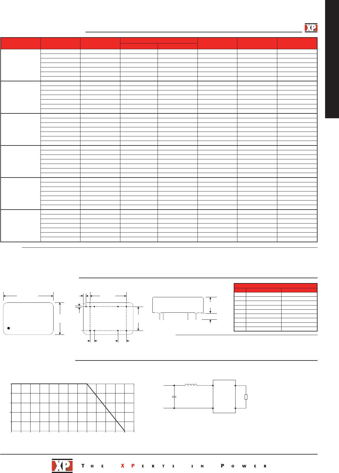
Operating Temperature • -40 °C to +100 °C, derate from 100% load
at +60 °C to no load at +100 °C
Case Temperature • +100 °C max
Storage Temperature • -40 °C to +125 °C
Humidity • Up to 95%, non-condensing
Cooling • Natural convection
EMC
Emissions • EN55022 Class A conducted and radiated
with external components - see
application note
ESD Immunity • EN61000-4-2, level 3, Perf Criteria A
EFT/Burst • EN61000-4-4, level 3, Perf Criteria A*
Surge • EN61000-4-5, installation class 3,
Perf Criteria A*
Conducted Immunity • EN61000-4-6, 10 Vrms, Perf Criteria A
Magnetic Field • EN61000-4-8, 1 A/m, Perf Criteria A
* A 330 µF, 100 V capacitor is required across input terminals to meet
performance criteria A.