NCP339
http://onsemi.com
9
APPLICATION INFORMATION
Power Dissipation
Main contributor in term of junction temperature is the
power dissipation of the power MOSFET. Assuming this,
the power dissipation and the junction temperature in
normal mode can be calculated with the following
equations:
• P
D
= R
DS(on)
× (I
OUT
)
2
P
D
= Power dissipation (W)
R
DS(on)
= Power MOSFET on resistance ()
I
OUT
= Output current (A)
• T
J
= P
D
× R
JA
+ T
A
T
J
= Junction temperature (°C)
R
JA
= Package thermal resistance (°C/W)
T
A
= Ambient temperature (°C)
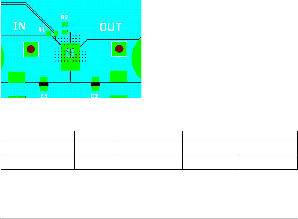
PCB Recommendations
The NCP339 integrates an up to 3 A rated PMOS FET, and
the PCB design rules must be respected to properly
evacuate the heat out of the silicon. By increasing PCB
area, especially around IN and OUT pins, the R
JA
of the
package can be decreased, allowing higher power
dissipation.
Routing example: 2 oz, 4 layers with vias across 2 internal
inners.
Figure 9.
Example of application definition.
T
J
− T
A
= R
JA
× P
D
= R
JA
× R
DSON
× I
2
T
J
: junction temperature.
T
A
: ambient temperature.
R
= Thermal resistance between IC and air, through PCB.
R
DSON
: intrinsic resistance of the IC Mosfet.
I: load DC current.
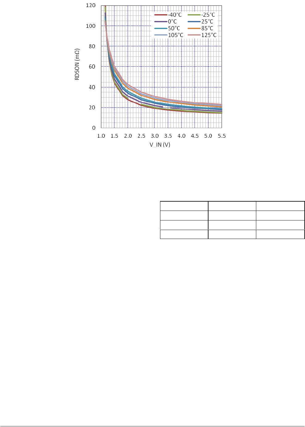
Taking into account of R
obtain with:
• 1 oz, 2 layers: 100°C/W.
At 3 A, 25°C ambient temperature, R
DSON
20 m @
Vin 5 V, the junction temperature will be:
T
J
= T
A
+ R
× P
D
= 25 + (0.02 × 3
2
) × 100 = 43°C
Taking into account of R
obtain with:
• 2 oz, 4 layers: 60°C/W.
At 3 A, 65°C ambient temperature, R
DSON
24 m @
Vin 5 V, the junction temperature will be:
T
J
= T
A
+ R
× P
D
= 65 + (0.024 × 3
2
) × 60 = 78°C
ORDERING INFORMATION
Device Marking Option Package Shipping
†
NCP339AFCT2G NP Without Auto−discharge WLCSP6, 1 x 1.5 mm
(Pb−Free)
3000 / Tape & Reel
NCP339BFCT2G DP With Auto−discharge WLCSP6, 1 x 1.5 mm
(Pb−Free)
3000 / Tape & Reel
†For information on tape and reel specifications, including part orientation and tape sizes, please refer to our Tape and Reel Packaging
Specifications Brochure, BRD8011/D.