LTC6078/LTC6079
4
60789fa
ELECTRICAL CHARACTERISTICS
The denotes the specifi cations which apply over the full operating
temperature range, otherwise specifi cations are at T
A
= 25°C. Test conditions are V
+
= 3V, V
= 0V, V
CM
= 0.5V unless otherwise noted.
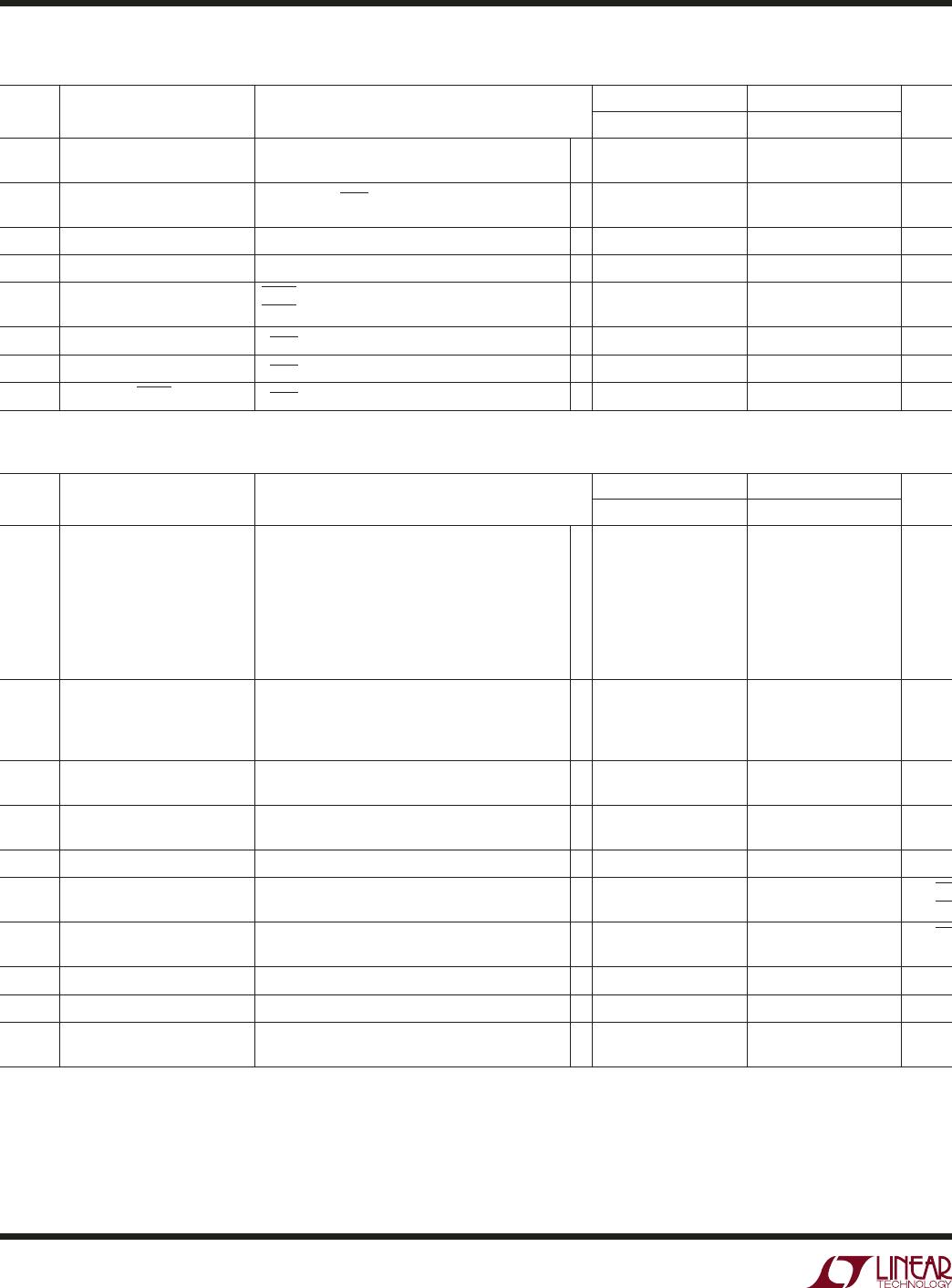
SYMBOL PARAMETER CONDITIONS C, I SUFFIXES H SUFFIX UNITS
MIN TYP MAX MIN TYP MAX
I
S
Supply Current
(per Amplifi er)
No Load
54 72
78
54 72
80
μA
μA
Shutdown Current
(per Amplifi er)
Shutdown, V
SHDN
≤ 0.8V, LTC6078DD
0.3 1 μA
V
S
Supply Voltage Range Guaranteed by the PSRR Test
2.7 5.5 2.7 5.5 V
Channel Separation f
s
= 10kHz, R
L
= 10k –110 –110 dB
Shutdown Logic SHDN High, LTC6078DD
SHDN Low, LTC6078DD
2
0.8
2
0.8
V
V
t
ON
Turn on Time V
SHDN
= 0.8V to 2V, LTC6078DD 50 50 µs
t
OFF
Turn off Time V
SHDN
= 2V to 0.8V, LTC6078DD 2 2 µs
Leakage of SHDN Pin V
SHDN
= 0V, LTC6078DD 0.6 μA
The denotes the specifi cations which apply over the full operating temperature range, otherwise specifi cations are at T
A
= 25°C. Test
conditions are V
+
= 5V, V
= 0V, V
CM
= 0.5V unless otherwise noted.
SYMBOL PARAMETER CONDITIONS C, I SUFFIXES H SUFFIX UNITS
MIN TYP MAX MIN TYP MAX
V
OS
Offset Voltage LTC6078MS8, LTC6078AMS8, LTC6079GN
V
CM
= 0.5V
LTC6078DD, LTC6079DHC V
CM
= 0.5V
LTC6078AMS8 V
CM
= 0.5V
LTC6078MS8 V
CM
= 0.5V
LTC6079GN V
CM
= 0.5V
LTC6078DD V
CM
= 0.5V
LTC6079DHC V
CM
= 0.5V
±10
±10
±20
±25
±30
±30
±35
±30
±35
±75
±102
±120
±125
±155
±10
±25
±30
±35
±30
±100
±140
±170
μV
μV
μV
μV
μV
μV
μV
ΔV
OS
ΔT Input Offset Voltage Drift
(Note 7)
LTC6078AMS8
LTC6078MS8
LTC6078DD, LTC6079GN
LTC6079DHC
±0.2
±0.3
±0.3
±0.7
±1.1
±1.4
±1.8
±0.2
±0.3
±0.7
±1.1
±1.4
μV/°C
μV/°C
μV/°C
μV/°C
I
B
Input Bias Current V
CM
= V
+
/2
V
CM
= V
+
/2
0.2
10
1
50
0.2
150
1
350
pA
pA
I
OS
Input Offset Current V
CM
= V
+
/2
V
CM
= V
+
/2
0.1
0.5 25
0.1
10 100
pA
pA
e
n
Input Noise Voltage 0.1Hz to 10Hz 1 1 µV
P-P
Input Noise Voltage Density f = 1kHz
f = 10kHz
18
16
18
16
nV/√Hz
nV/√Hz
i
n
Input Noise Current Density
(Note 8)
0.56 0.56 fA/√Hz
Input Common Mode Range
V
V
+
V
V
+
V
C
DIFF
Differential Input Capacitance 10 10 pF
C
CM
Common Mode Input
Capacitance
18 18 pF
LTC6078/LTC6079
5
60789fa
Note 1: Stresses beyond those listed under Absolute Maximum Ratings
may cause permanent damage to the device. Exposure to any Absolute
Maximum Rating condition for extended periods may affect device
reliability and lifetime.
Note 2: A heat sink may be required to keep the junction temperature
below the absolute maximum. This depends on the power supply voltage
and how many amplifi ers are shorted.
Note 3: The LTC6078C/LTC6079C and LTC6078I/LTC6079I are guaranteed
functional over the operating temperature range of –40°C to 85°C. The
LTC6078H/LTC6079H are guaranteed functional over the operating
temperature range of –40°C to 125°C.
Note 4: The LTC6078C/LTC6079C are guaranteed to meet specifi ed
SYMBOL PARAMETER CONDITIONS C, I SUFFIXES H SUFFIX UNITS
MIN TYP MAX MIN TYP MAX
CMRR Common Mode Rejection
Ratio
All Packages V
CM
= 0V to 5V
LTC6078AMS8 V
CM
= 0V to 5V
LTC6078AMS8 V
CM
= 0V to 3.7V
LTC6078MS8 V
CM
= 0V to 5V
LTC6078MS8 V
CM
= 0V to 3.7V
LTC6079GN V
CM
= 0V to 5V
LTC6079GN V
CM
= 0V to 3.7V
LTC6078DD, LTC6079DHC V
CM
= 0V to 5V
LTC6078DD, LTC6079DHC V
CM
= 0V to 3.7V
91
90
94
88
90
86
90
86
90
105
105
105
100
105
100
105
100
105
91
90
94
88
90
86
90
105
105
105
100
105
100
105
dB
dB
dB
dB
dB
dB
dB
dB
dB
PSRR Power Supply Rejection Ratio V
S
= 2.7V to 5.5V
100
97
120
97
120 dB
dB
V
OUT
Output Voltage, High
(Referred to V
+
)
No Load
I
SOURCE
= 0.5mA
I
SOURCE
= 5mA
50
500
2
20
200
55
550
2
20
200
mV
mV
mV
Output Voltage, Low
(Referred to V
)
No Load
I
SINK
= 0.5mA
I
SINK
= 5mA
1
15
150
40
400
1
15
150
45
450
mV
mV
mV
A
VOL
Large-Signal Voltage Gain R
LOAD
= 10k, 0.5V ≤ V
OUT
≤ 4.5V
115 130 110 125 dB
I
SC
Output Short-Circuit Current Source
Sink
14
14
25
25
12
12
25
25
mA
mA
SR Slew Rate A
V
= 1 0.05 0.05 V/μs
GBW Gain-Bandwidth Product
(f
TEST
= 10kHz)
R
L
= 100k
420
360
750 420
320
750 kHz
kHz
Φ
0
Phase Margin R
L
= 10k, C
L
= 200pF 66 66 Deg
t
S
Settling Time 0.1% A
V
= 1, 1V Step 24 24 μs
I
S
Supply Current
(per Amplifi er)
No Load
55 74
82
55 74
84
μA
μA
Shutdown Current
(per Amplifi er)
Shutdown, V
SHDN
≤ 1.2V, LTC6078DD
1.5 5 1.5 5 μA
V
S
Supply Voltage Range Guaranteed by the PSRR Test
2.7 5.5 2.7 5.5 V
Channel Separation f
s
= 10kHz, R
L
= 10k –110 –110 dB
Shutdown Logic SHDN High, LTC6078DD
SHDN Low, LTC6078DD
3.5
1.2
3.5
1.2
V
V
t
ON
Turn on Time V
SHDN
= 1.2V to 3.5V, LTC6078DD 50 50 µs
t
OFF
Turn off Time V
SHDN
= 1.2V to 3.5V, LTC6078DD 2 2 µs
Leakage of SHDN Pin V
SHDN
= 0V, LTC6078DD 0.6 μA
performance from 0°C to 70°C. The LTC6078C/LTC6079C are designed,
characterized and expected to meet specifi ed performance from –40°C
to 85°C but are not tested or QA sampled at these temperatures. The
LTC6078I/LTC6079I are guaranteed to meet specifi ed performance from
–40°C to 85°C. The LTC6078H/LTC6079H are guaranteed to meet specifi ed
performance from –40°C to 125°C.
Note 5: V
OS
and V
OS
drift are 100% tested at 25°C and 125°C.
Note 6: I
B
and I
OS
are guaranteed by the V
S
= 5V test.
Note 7: V
OS
drift is guaranteed by the V
S
= 3V test.
Note 8: Current noise is calculated from i
n
= √2qI
B
, where q = 1.6 • 10
–19
coulomb.
ELECTRICAL CHARACTERISTICS
The denotes the specifi cations which apply over the full operating
temperature range, otherwise specifi cations are at T
A
= 25°C. Test conditions are V
+
= 5V, V
= 0V, V
CM
= 0.5V unless otherwise noted.
LTC6078/LTC6079
6
60789fa
NUMBER OF AMPS OUT OF 200
14
12
10
6
8
4
2
0
60789 G01
–11 7–9 –7 –5 1 5 9–3 –1 3
V
OS
(µV)
LTC6078MS8
V
S
= 3V
V
CM
= 0.5V
T
A
= 25°C
TIME (5s/DIV)
60789 G09
V
S
= 5V
V
CM
= 0.5V
VOLTAGE NOISE (500nV/DIV)
V
CM
(V)
0
INPUT BIAS CURRENT (pA)
400
300
200
100
–0
–100
–200
–300
–400
4
1
2
3
5
60789 G07
V
S
= 5V
T
A
= 125°C
FREQUENCY (Hz)
NOISE VOLTAGE (nV/Hz)
90
80
70
60
50
40
30
20
10
0
1 100 1k 100k
60789 G08
10 10k
V
S
= 5V
V
CM
= 0.5V
V
S
= 3V
V
CM
= 0.5V
TEMPERATURE (°C)
0
INPUT BIAS CURRENT (pA)
180
160
140
100
120
20
40
60
80
0
100
60789 G05
25 50 75 125
V
S
= 5V
V
CM
= 2.5V
V
CM
(V)
0
INPUT BIAS CURRENT (pA)
30
24
18
12
6
–0
–6
–12
–18
–24
–30
4
1
2
3
5
60789 G06
V
S
= 5V
T
A
= 70°C
T
A
= 85°C
µV/°C
NUMBER OF AMPS OUT OF 200
50
45
40
30
35
25
20
15
10
5
0
60789 G04
–0.8 0.6–0.6 –0.4 0 0.4 0.8–0.2 0.2
LTC6078MS8
V
S
= 3V
V
CM
= 0.5V
T
A
= –40°C TO 125°C
V
CM
(V)
0
V
OS
(µV)
1.5
2.5
60789 G03
0.5 1.0 2.0
3.5
4.5
4.0
100
40
20
80
60
0
–20
–100
–40
–60
–80
5.03.0
V
S
= 5V
T
A
= 25°C
REPRESENTATIVE PARTS
V
CM
(V)
0
V
OS
(µV)
1.5
2.5
60789 G02
0.5 1.0 2.0
40
30
20
10
0
–10
–20
–30
–40
3.0
V
S
= 3V
T
A
= 25°C
REPRESENTATIVE PARTS
V
OS
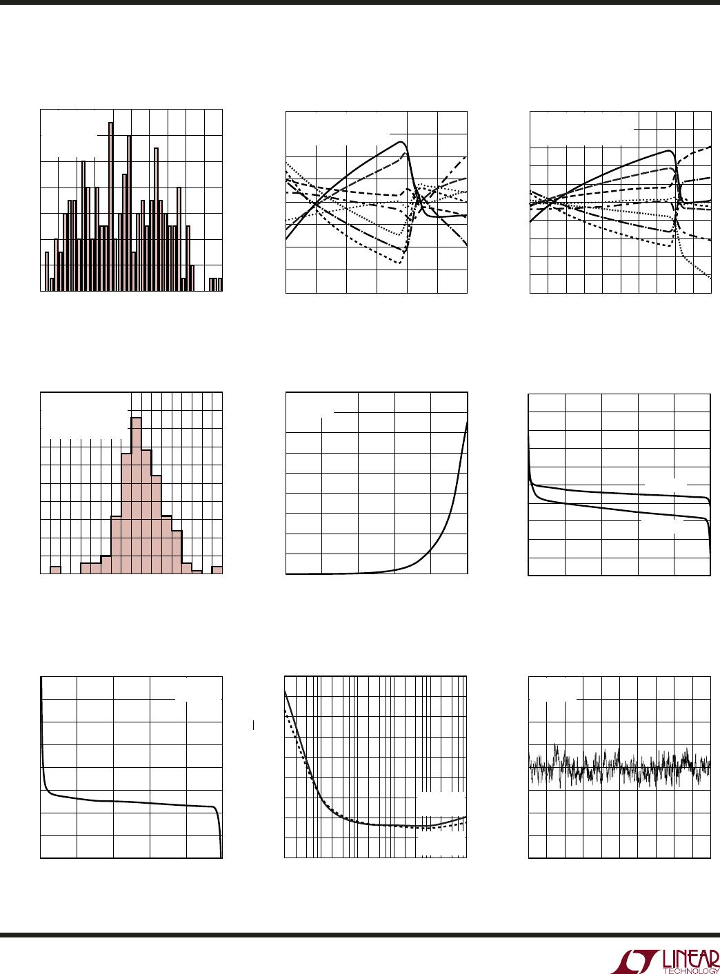
Drift Distribution
Input Bias vs Temperature Input Bias vs V
CM
Input Bias vs V
CM
Voltage Noise Spectrum
0.1Hz to 10Hz Output Voltage
Noise
V
OS
Distribution
V
OS
vs V
CM
V
OS
vs V
CM
TYPICAL PERFOR A CE CHARACTERISTICS
UW

LTC6078AHMS8#TRPBF

Mfr. #:
Manufacturer:
Analog Devices Inc.
Description:
Precision Amplifiers Dual Micropower Precision R-R In/Out CMOS Op Amp
Lifecycle:
New from this manufacturer.
Delivery:
DHL FedEx Ups TNT EMS
Payment:
T/T Paypal Visa MoneyGram Western Union