LTC6078/LTC6079
10
60789fa
APPLICATIO S I FOR ATIO
WUU
U
PC Board Layout
Mechanical stress on a PC board and soldering-induced
stress can cause the V
OS
and V
OS
drift to shift. The DD
and DHC packages are more sensitive to stress. A simple
way to reduce the stress-related shifts is to mount the IC
near the short edge of the PC board, or in a corner. The
board edge acts as a stress boundary, or a region where
the fl exure of the board is minimum. The package should
always be mounted so that the leads absorb the stress and
not the package. The package is generally aligned with the
leads paralled to the long side of the PC board.
The most effective technique to relieve the PC board stress
is to cut slots in the board around the op amp. These slots
can be cut on three sides of the IC and the leads can exit on
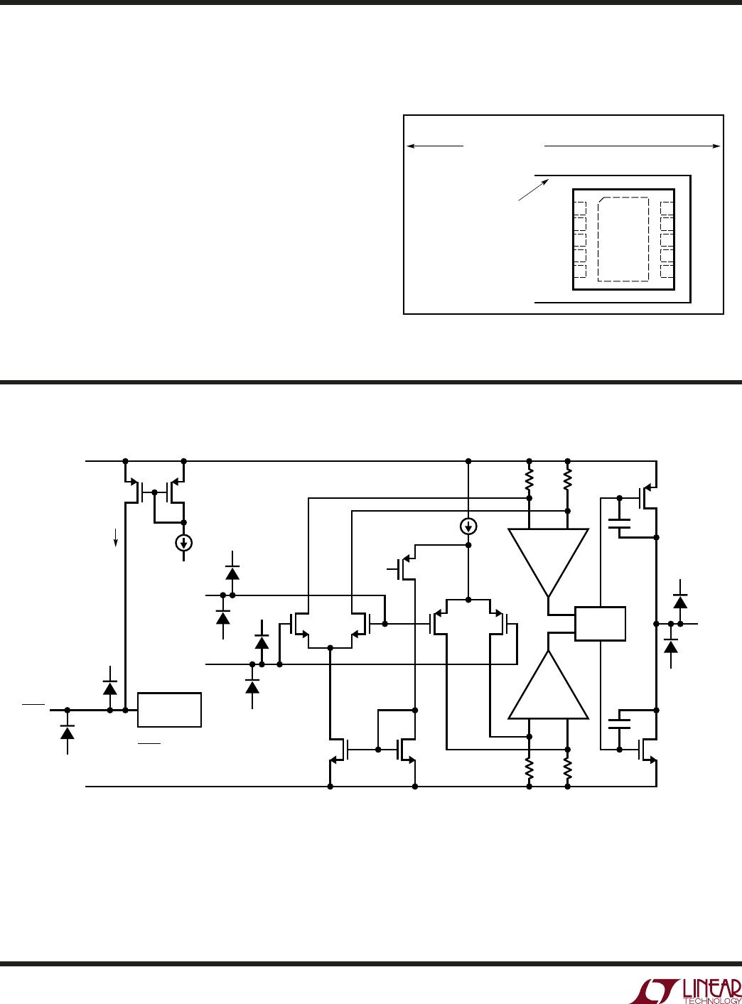
the fourth side. Figure 3 shows the layout of a LTC6078DD
with slots at three sides.
Figure 3. Vertical Orientation of LTC6078DD with Slots
60789 F03
LONG DIMENSION
SLOTS
Simplifi ed Schematic of the Amplifi er
R1 R2
R3
V
+
V
–
R4
–
+
D8
D7
OUT
M8
M9
C1
C2
60789 SS
V
+
V
–
D5
D6
–
+
OUTPUT
CONTROL
M4
M6
A1
A2
M7
M5
I1
V
BIAS
M1 M2
M3
–IN
V
+
V
–
V
+
V
–
D3
D4
+IN
V
–
M11M10
1µA
I2
V
+
V
–
D1
D2
SHDN
BIAS
GENERATION
NOTE: SHDN IS ONLY AVAILABLE
IN THE DFN10 PACKAGE
SCHE ATIC
WW
SI PLIFIED

