LTC6078/LTC6079
1
60789fa
Micropower Precision,
Dual/Quad CMOS
Rail-to-Rail Input/Output Amplifi ers
The LTC
®
6078/LTC6079 are dual/quad, low offset, low
noise operational amplifi ers with low power consumption
and rail-to-rail input/output swing.
Input offset voltage is trimmed to less than 25µV and the
CMOS inputs draw less than 50pA of bias current. The low
offset drift, excellent CMRR, and high voltage gain make
it a good choice for precision signal conditioning.
Each amplifi er draws only 54µA current on a 3V supply. The
micropower, rail-to-rail operation of the LTC6078/LTC6079
is well suited for portable instruments and single supply
applications.
The LTC6078/LTC6079 are specifi ed on power supply
voltages of 3V and 5V from –40 to 125°C. The dual am-
plifi er LTC6078 is available in 8-lead MSOP and 10-lead
DFN packages. The quad amplifi er LTC6079 is available
in 16-lead SSOP and DFN packages.
Photodiode Amplifi er
High Impedance Sensor Amplifi er
Microvolt Accuracy Threshold Detection
Instrumentation Amplifi ers
Battery Powered Applications
Maximum Offset Voltage of 25µV (25°C)
Maximum Offset Drift of 0.7µV/°C
Maximum Input Bias:
1pA (25°C)
50pA (≤85°C)
Micropower: 54µA per Amp
95dB CMRR (Min)
100dB PSRR (Min)
Input Noise Voltage Density: 16nV/√Hz
Rail-to-Rail Inputs and Outputs
2.7V to 5.5V Operation Voltage
LTC6078 Available in 8-Lead MSOP and 10-Lead DFN
Packages; LTC6079 Available in 16-Lead SSOP and
DFN Packages
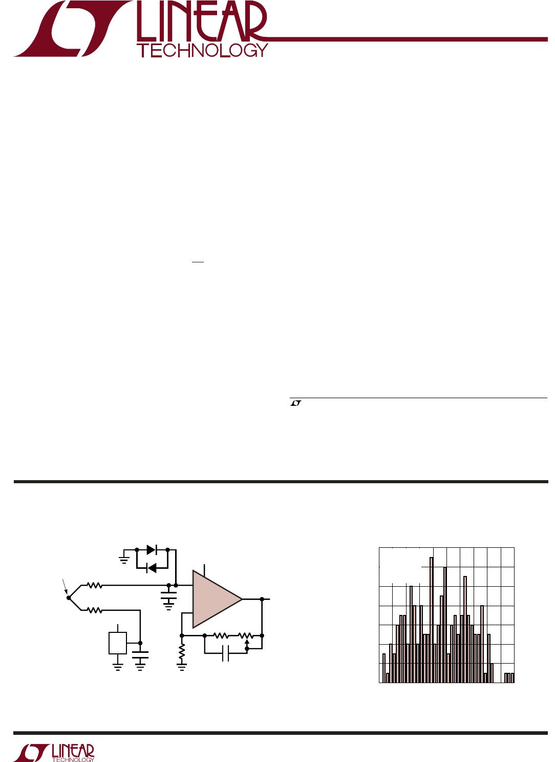
Thermocouple Signal Conditioner
APPLICATIO S
U
FEATURES
DESCRIPTIO
U
TYPICAL APPLICATIO
U
, LT, LTC and LTM are registered trademarks of Linear Technology Corporation.
All other trademarks are the property of their respective owners. Patent Pending.
1k
5.6pF
0.1µF
OUT = 10mV/°C
0°C TO 500°C ±0.5°C
5V
5V
+
60789 TA01a
2.49M
SMT
1/4W
150k
NORMALLY
FLOATING
OMEGA
5TC-TT-K-30-36
THERMOCOUPLE
AMPLIFIER PROTECTED TO ±190V, ACCIDENTAL CONTACT
40.6µV/°C
SMT
1/4W
150k
10k
100pF
K
1/2
LTC6078
LT1025
V
OS
Distribution
V
OS
(µV)
NUMBER OF AMPS OUT OF 200
14
12
10
6
8
4
2
0
60789 TA01b
–11 7–9 –7 –5 1 5 9–3 –1 3
LTC6078MS8
V
S
= 3V
V
CM
= 0.5V
T
A
= 25°C
LTC6078/LTC6079
2
60789fa
Total Supply Voltage (V
+
to V
) ...................................6V
Input Voltage ...................................................... V
to V
+
Output Short Circuit Duration (Note 2) ............ Indefi nite
Operating Temperature Range (Note 3)
LTC6078C, LTC6079C .......................... –40°C to 85°C
LTC6078I, LTC6079I ............................ –40°C to 85°C
LTC6078H, LTC6079H ........................ –40°C to 125°C
(Not Available in DFN Package)
(Note 1)
Specifi ed Temperature Range (Note 4)
LTC6078C, LTC6079C .............................. 0°C to 70°C
LTC6078I, LTC6079I ............................ –40°C to 85°C
LTC6078H, LTC6079H ........................ –40°C to 125°C
Junction Temperature
DFN Packages ................................................... 125°C
All Other Packages ............................................ 150°C
Storage Temperature Range
DFN Packages .................................... –65°C to 125°C
All Other Packages ............................. –65°C to 150°C
Lead Temperature (Soldering, 10 Sec) .................. 300°C
ABSOLUTE AXI U RATI GS
W
WW
U
PACKAGE/ORDER I FOR ATIO
UUW
TOP VIEW
DD PACKAGE
10-LEAD (3mm × 3mm) PLASTIC DFN
10
9
6
7
8
4
5
3
2
1
V
+
OUTB
–INB
+INB
SHDN_B
OUTA
–INA
+INA
V
SHDN_A
B
A
T
JMAX
= 125°C, θ
JA
= 43°C/W
UNDERSIDE METAL CONNECTED TO V
1
2
3
4
OUTA
–INA
+INA
V
8
7
6
5
V
+
OUTB
–INB
+INB
TOP VIEW
MS8 PACKAGE
8-LEAD PLASTIC MSOP
B
A
T
JMAX
= 150°C, θ
JA
= 200°C/W
ORDER PART
NUMBER
DD PART
MARKING*
LTC6078CDD
LTC6078IDD
LBBB
LBBB
ORDER PART
NUMBER
MS8 PART
MARKING*
LTC6078ACMS8
LTC6078CMS8
LTC6078AIMS8
LTC6078IMS8
LTC6078AHMS8
LTC6078HMS8
LTAJZ
LTAJZ
LTAJZ
LTAJZ
LTAJZ
LTAJZ
16
15
14
13
12
11
10
9
1
2
3
4
5
6
7
8
OUTD
–IND
+IND
V
+INC
–INC
OUTC
NC
OUTA
–INA
+INA
V
+
+INB
–INB
OUTB
NC
TOP VIEW
DHC PACKAGE
16-LEAD (5mm × 3mm) PLASTIC DFN
D
A
C
B
T
JMAX
= 125°C, θ
JA
= 43°C/W
UNDERSIDE METAL CONNECTED TO V
GN PACKAGE
16-LEAD PLASTIC SSOP
1
2
3
4
5
6
7
8
TOP VIEW
16
15
14
13
12
11
10
9
OUTA
–INA
+INA
V
+
+INB
–INB
OUTB
NC
OUTD
–IND
+IND
V
+INC
–INC
OUTC
NC
D
A
C
B
T
JMAX
= 150°C, θ
JA
= 110°C/W
ORDER PART
NUMBER
DHC PART
MARKING*
LTC6079CDHC
LTC6079IDHC
6079
6079
ORDER PART
NUMBER
GN PART
MARKING
LTC6079CGN
LTC6079IGN
LTC6079HGN
6079
6079I
6079H
Order Options Tape and Reel: Add #TR
Lead Free: Add #PBF Lead Free Tape and Reel: Add #TRPBF
Lead Free Part Marking: http://www.linear.com/leadfree/
Consult LTC Marketing for parts specifi ed with wider operating temperature ranges.
*The temperature grades and parametric grades are identifi ed by a label on the shipping container.
LTC6078/LTC6079
3
60789fa
The denotes the specifi cations which apply over the full operating
temperature range, otherwise specifi cations are at T
A
= 25°C. Test conditions are V
+
= 3V, V
= 0V, V
CM
= 0.5V unless otherwise noted.
SYMBOL PARAMETER CONDITIONS C, I SUFFIXES H SUFFIX UNITS
MIN TYP MAX MIN TYP MAX
V
OS
Offset Voltage (Note 5) LTC6078MS8, LTC6078AMS8, LTC6079GN
V
CM
= 0.5V, 2.5V
LTC6078DD, LTC6079DHC V
CM
= 0.5V, 2.5V
LTC6078AMS8 V
CM
= 0.5V
LTC6078MS8 V
CM
= 0.5V
LTC6079GN V
CM
= 0.5V
LTC6078DD V
CM
= 0.5V
LTC6079DHC V
CM
= 0.5V
±7
±7
±20
±25
±30
±30
±35
±25
±30
±70
±97
±115
±120
±150
±7
±25
±30
±35
±25
±95
±135
±165
μV
μV
μV
μV
μV
μV
μV
ΔV
OS
ΔT Input Offset Voltage Drift
(Note 5)
LTC6078AMS8
LTC6078MS8
LTC6078DD, LTC6079GN
LTC6079DHC
±0.2
±0.3
±0.3
±0.7
±1.1
±1.4
±1.8
±0.2
±0.3
±0.7
±1.1
±1.4
μV/°C
μV/°C
μV/°C
μV/°C
I
B
Input Bias Current
(Note 6)
V
CM
= V
+
/2
V
CM
= V
+
/2
0.2
10
1
50
0.2
150
1
350
pA
pA
I
OS
Input Offset Current
(Note 6)
V
CM
= V
+
/2
V
CM
= V
+
/2
0.1
0.5 25
0.1
10 100
pA
pA
e
n
Input Noise Voltage 0.1Hz to 10Hz 1 1 µV
P-P
Input Noise Voltage Density f = 1kHz
f = 10kHz
18
16
18
16
nV/√Hz
nV/√Hz
i
n
Input Noise Current Density
(Note 8)
0.56 0.56 fA/√Hz
Input Common Mode Range
V
V
+
V
V
+
V
C
DIFF
Differential Input Capacitance 10 10 pF
C
CM
Common Mode Input
Capacitance
18 18 pF
CMRR Common Mode Rejection
Ratio
All Packages V
CM
= 0V to 3V
LTC6078AMS8 V
CM
= 0V to 3V
LTC6078AMS8 V
CM
= 0V to 1.7V
LTC6078MS8 V
CM
= 0V to 3V
LTC6078MS8 V
CM
= 0V to 1.7V
LTC6079GN V
CM
= 0V to 3V
LTC6079GN V
CM
= 0V to 1.7V
LTC6078DD, LTC6079DHC V
CM
= 0V to 3V
LTC6078DD, LTC6079DHC V
CM
= 0V to 1.7V
95
87
91
85
89
84
88
83
87
110
105
103
102
102
102
102
100
102
95
87
91
85
89
84
88
110
103
103
100
102
100
102
dB
dB
dB
dB
dB
dB
dB
dB
dB
PSRR Power Supply Rejection Ratio V
S
= 2.7V to 5.5V
100
97
120 100
97
120 dB
dB
V
OUT
Output Voltage, High
(Referred to V
+
)
No Load
I
SOURCE
= 0.2mA
I
SOURCE
= 2mA
35
350
1
15
150
40
400
1
15
150
mV
mV
mV
Output Voltage, Low
(Referred to V
)
No Load
I
SINK
= 0.2mA
I
SINK
= 2mA
1
10
100
30
300
1
10
100
35
350
mV
mV
mV
A
VOL
Large-Signal Voltage Gain R
LOAD
= 10k, 0.5V ≤ V
OUT
≤ 2.5V
115 130 110 125 dB
I
SC
Output Short-Circuit Current Source
Sink
5
7
10
14
4
6
10
14
mA
mA
SR Slew Rate A
V
= 1 0.05 0.05 V/μs
GBW Gain-Bandwidth Product
(f
TEST
= 10kHz)
R
L
= 100k
420
360
750 420
320
750 kHz
kHz
Φ
0
Phase Margin R
L
= 10k, C
L
= 200pF 66 66 Deg
t
S
Settling Time 0.1% A
V
= 1, 1V Step 24 24 μs
ELECTRICAL CHARACTERISTICS

LTC6079IGN#TRPBF

Mfr. #:
Manufacturer:
Analog Devices Inc.
Description:
Precision Amplifiers Quad Micropower Precision R-R In/Out CMOS Op Amp
Lifecycle:
New from this manufacturer.
Delivery:
DHL FedEx Ups TNT EMS
Payment:
T/T Paypal Visa MoneyGram Western Union