©2012 Silicon Storage Technology, Inc. DS25023B 06/13
7
1 Mbit / 2 Mbit / 4 Mbit Multi-Purpose Flash
SST39LF010 / SST39LF020 / SST39LF040
SST39VF010 / SST39VF020 / SST39VF040
Data Sheet
internal Erase operation, the only valid read is Toggle Bit or Data# Polling. See Table 4 for the com-
mand sequence, Figure 10 for timing diagram, and Figure 18 for the flowchart. Any commands written
during the Chip-Erase operation will be ignored.
Write Operation Status Detection
The SST39LF010/020/040 and SST39VF010/020/040 devices provide two software means to detect
the completion of a Write (Program or Erase) cycle, in order to optimize the system write cycle time.
The software detection includes two status bits: Data# Polling (DQ
7
) and Toggle Bit (DQ
6
). The End-of-
Write detection mode is enabled after the rising edge of WE# which initiates the internal Program or
Erase operation.
The actual completion of the nonvolatile write is asynchronous with the system; therefore, either a
Data# Polling or Toggle Bit read may be simultaneous with the completion of the Write cycle. If this
occurs, the system may possibly get an erroneous result, i.e., valid data may appear to conflict with
either DQ
7
or DQ
6
. In order to prevent spurious rejection, if an erroneous result occurs, the software
routine should include a loop to read the accessed location an additional two (2) times. If both reads
are valid, then the device has completed the Write cycle, otherwise the rejection is valid.
©2012 Silicon Storage Technology, Inc. DS25023B 06/13
8
1 Mbit / 2 Mbit / 4 Mbit Multi-Purpose Flash
SST39LF010 / SST39LF020 / SST39LF040
SST39VF010 / SST39VF020 / SST39VF040
Data Sheet
Data# Polling (DQ
7
)
When the SST39LF010/020/040 and SST39VF010/020/040 are in the internal Program operation, any
attempt to read DQ
7
will produce the complement of the true data. Once the Program operation is
completed, DQ
7
will produce true data. Note that even though DQ
7
may have valid data immediately
following completion of an internal Write operation, the remaining data outputs may still be invalid: valid
data on the entire data bus will appear in subsequent successive Read cycles after an interval of 1 µs.
During internal Erase operation, any attempt to read DQ
7
will produce a “0”. Once the internal Erase
operation is completed, DQ
7
will produce a “1”. The Data# Polling is valid after the rising edge of fourth
WE# (or CE#) pulse for Program operation. For Sector- or Chip-Erase, the Data# Polling is valid after
the rising edge of sixth WE# (or CE#) pulse. See Figure 7 for Data# Polling timing diagram and Figure
16 for a flowchart.
Toggle Bit (DQ
6
)
During the internal Program or Erase operation, any consecutive attempts to read DQ
6
will produce
alternating ‘0’s and ‘1’s, i.e., toggling between 0 and 1. When the internal Program or Erase operation
is completed, the toggling will stop. The device is then ready for the next operation. The Toggle Bit is
valid after the rising edge of fourth WE# (or CE#) pulse for Program operation. For Sector- or Chip-
Erase, the Toggle Bit is valid after the rising edge of sixth WE# (or CE#) pulse. See Figure 8 for Toggle
Bit timing diagram and Figure 16 for a flowchart.
Data Protection
The SST39LF010/020/040 and SST39VF010/020/040 provide both hardware and software features to
protect nonvolatile data from inadvertent writes.
Hardware Data Protection
Noise/Glitch Protection: A WE# or CE# pulse of less than 5 ns will not initiate a Write cycle.
V
DD
Power Up/Down Detection: The Write operation is inhibited when V
DD
is less than 1.5V.
Write Inhibit Mode:
Forcing OE# low, CE# high, or WE# high will inhibit the Write operation. This pre-
vents inadvertent writes during power-up or power-down.
©2012 Silicon Storage Technology, Inc. DS25023B 06/13
9
1 Mbit / 2 Mbit / 4 Mbit Multi-Purpose Flash
SST39LF010 / SST39LF020 / SST39LF040
SST39VF010 / SST39VF020 / SST39VF040
Data Sheet
Software Data Protection (SDP)
The SST39LF010/020/040 and SST39VF010/020/040 provide the JEDEC approved Software Data
Protection scheme for all data alteration operation, i.e., Program and Erase. Any Program operation
requires the inclusion of a series of three-byte sequence. The three-byte load sequence is used to ini-
tiate the Program operation, providing optimal protection from inadvertent Write operations, e.g., dur-
ing the system power-up or power-down. Any Erase operation requires the inclusion of six-byte load
sequence. These devices are shipped with the Software Data Protection permanently enabled. See
Table 4 for the specific software command codes. During SDP command sequence, invalid commands
will abort the device to read mode, within T
RC.
Product Identification
The Product Identification mode identifies the devices as the SST39LF/VF010, SST39LF/VF020, and
SST39LF/VF040 and manufacturer as SST. This mode may be accessed by software operations.
Users may use the Software Product Identification operation to identify the part (i.e., using the device
ID) when using multiple manufacturers in the same socket. For details, see Table 4 for software opera-
tion, Figure 11 for the Software ID Entry and Read timing diagram, and Figure 17 for the Software ID
entry command sequence flowchart.
Product Identification Mode Exit/Reset
In order to return to the standard Read mode, the Software Product Identification mode must be exited.
Exit is accomplished by issuing the Software ID Exit command sequence, which returns the device to
the Read operation. Please note that the Software ID Exit command is ignored during an internal Pro-
gram or Erase operation. See Table 4 for software command codes, Figure 12 for timing waveform,
and Figure 17 for a flowchart.
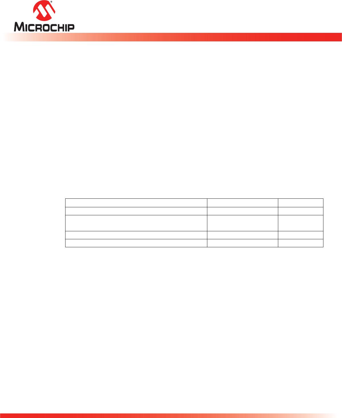
Table 2: Product Identification
Address Data
Manufacturer’s ID 0000H BFH
Device ID
SST39LF/VF010 0001H D5H
SST39LF/VF020 0001H D6H
SST39LF/VF040 0001H D7H
T2.1 25023

SST39VF020-70-4I-NHE

Mfr. #:
Manufacturer:
Microchip Technology
Description:
NOR Flash 256K X 8 70ns
Lifecycle:
New from this manufacturer.
Delivery:
DHL FedEx Ups TNT EMS
Payment:
T/T Paypal Visa MoneyGram Western Union