NXP Semiconductors
PMN42XPEA
20 V, P-channel Trench MOSFET
PMN42XPEA All information provided in this document is subject to legal disclaimers. © NXP Semiconductors N.V. 2014. All rights reserved
Product data sheet 21 March 2014 6 / 15
10. Characteristics
Table 7. Characteristics
Symbol Parameter Conditions Min Typ Max Unit
Static characteristics
V
(BR)DSS
drain-source
breakdown voltage
I
D
= -250 µA; V
GS
= 0 V; T
j
= 25 °C -20 - - V
V
GSth
gate-source threshold
voltage
I
D
= -250 µA; V
DS
= V
GS
; T
j
= 25 °C -0.75 -1 -1.25 V
V
DS
= -20 V; V
GS
= 0 V; T
j
= 25 °C - - -1 µAI
DSS
drain leakage current
V
DS
= -20 V; V
GS
= 0 V; T
amb
= 150 °C - - -10 µA
V
GS
= 12 V; V
DS
= 0 V; T
j
= 25 °C - - 10 µAI
GSS
gate leakage current
V
GS
= -12 V; V
DS
= 0 V; T
j
= 25 °C - - -10 µA
V
GS
= -4.5 V; I
D
= -3 A; T
j
= 25 °C - 41 46
V
GS
= -4.5 V; I
D
= -3 A; T
j
= 150 °C - 56 64
R
DSon
drain-source on-state
resistance
V
GS
= -2.5 V; I
D
= -3 A; T
j
= 25 °C - 56 64
g
fs
forward
transconductance
V
DS
= -10 V; I
D
= -4 A; T
j
= 25 °C - 12.5 - S
Dynamic characteristics
Q
G(tot)
total gate charge - 11.5 17.3 nC
Q
GS
gate-source charge - 2.7 - nC
Q
GD
gate-drain charge
V
DS
= -10 V; I
D
= -4 A; V
GS
= -4.5 V;
T
j
= 25 °C
- 2.4 - nC
C
iss
input capacitance - 1410 - pF
C
oss
output capacitance - 207 - pF
C
rss
reverse transfer
capacitance
V
DS
= -10 V; f = 1 MHz; V
GS
= 0 V;
T
j
= 25 °C
- 148 - pF
t
d(on)
turn-on delay time - 17 - ns
t
r
rise time - 27 - ns
t
d(off)
turn-off delay time - 33 - ns
t
f
fall time
V
DS
= -10 V; I
D
= -4 A; V
GS
= -4.5 V;
R
G(ext)
= 6 Ω; T
j
= 25 °C
- 27 - ns
Source-drain diode
V
SD
source-drain voltage I
S
= -1.2 A; V
GS
= 0 V; T
j
= 25 °C - -0.7 -1.2 V
NXP Semiconductors
PMN42XPEA
20 V, P-channel Trench MOSFET
PMN42XPEA All information provided in this document is subject to legal disclaimers. © NXP Semiconductors N.V. 2014. All rights reserved
Product data sheet 21 March 2014 7 / 15
V
DS
(V)
0 -4-3-1 -2
aaa-004348
-8
-4
-12
-16
I
D
(A)
0
V
GS
= -2.5 V
-2.2 V
-8 V
-4.5 V
-3 V
-2 V
-1.8 V
T
j
= 25 °C
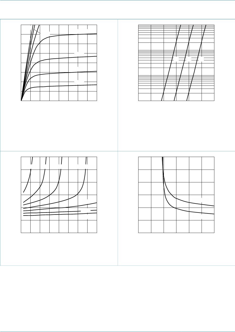
Fig. 6. Output characteristics: drain current as a
function of drain-source voltage; typical values
017aaa129
V
GS
(V)
0.0 - 1.5- 1.0- 0.5
- 10
- 4
- 10
- 5
- 10
- 3
I
D
(A)
- 10
- 6
(2)(1) (3)
T
j
= 25 °C; V
DS
= -3 V
(1) minimum values
(2) typical values
(3) maximum values
Fig. 7. Sub-threshold drain current as a function of
gate-source voltage
I
D
(A)
0 -16-12-4 -8
aaa-004349
50
100
150
R
DSon
(mΩ)
0
V
GS
= -2.5 V
-2.2 V
-8 V
-4.5 V
-3 V
-2 V-1.8 V
T
j
= 25 °C
Fig. 8. Drain-source on-state resistance as a function
of drain current; typical values
V
GS
(V)
0 -6-4-2
aaa-004350
50
100
150
R
DSon
(mΩ)
0
T
j
= 25 °C
T
j
= 150 °C
I
D
= -4 A
Fig. 9. Drain-source on-state resistance as a function
of gate-source voltage; typical values
NXP Semiconductors
PMN42XPEA
20 V, P-channel Trench MOSFET
PMN42XPEA All information provided in this document is subject to legal disclaimers. © NXP Semiconductors N.V. 2014. All rights reserved
Product data sheet 21 March 2014 8 / 15
V
GS
(V)
0 -4-3-1 -2
aaa-004351
-8
-4
-12
-16
I
D
(A)
0
T
j
= 25 °CT
j
= 150 °C
T
j
= 25 °C T
j
= 150 °C
V
DS
> I
D
× R
DSon
Fig. 10. Transfer characteristics: drain current as a
function of gate-source voltage; typical values
T
j
(°C)
-60 1801200 60
aaa-004352
1.00
0.75
1.25
1.50
a
0.50
Fig. 11. Normalized drain-source on-state resistance
as a function of junction temperature; typical
values
T
j
(°C)
-60 1801200 60
aaa-004353
-0.5
-1.0
-1.5
V
GS(th)
(V)
0.0
max
typ
min
I
D
= -0.25 mA; V
DS
= V
GS
Fig. 12. Gate-source threshold voltage as a function of
junction temperature
V
DS
(V)
-10
-1
-10
2
-10-1
aaa-004354
10
3
10
2
10
4
C
(pF)
10
C
iss
C
oss
C
rss
f = 1 MHz; V
GS
= 0 V
Fig. 13. Input, output and reverse transfer capacitances
as a function of drain-source voltage; typical
values

PMN42XPEAX

Mfr. #:
Manufacturer:
Nexperia
Description:
MOSFET 20V P-channel Trench MOSFET
Lifecycle:
New from this manufacturer.
Delivery:
DHL FedEx Ups TNT EMS
Payment:
T/T Paypal Visa MoneyGram Western Union

Products related to this Datasheet