MC74HCT4051A, MC74HCT4052A, MC74HCT4053A
http://onsemi.com
4
RECOMMENDED OPERATING CONDITIONS
Symbol Parameter Min Max Unit
V
CC
Positive DC Supply Voltage (Referenced to GND)
(Referenced to V
EE
)
2.0
2.0
6.0
12.0
V
V
EE
Negative DC Supply Voltage, Output (Referenced to
GND)
−6.0 GND V
V
IS
Analog Input Voltage V
EE
V
CC
V
V
in
Digital Input Voltage (Referenced to GND) GND V
CC
V
V
IO
* Static or Dynamic Voltage Across Switch 1.2 V
T
A
Operating Temperature Range, All Package Types −55 +125 °C
t
r
, t
f
Input Rise/Fall Time V
CC
= 2.0 V
(Channel Select or Enable Inputs) V
CC
= 3.0 V
V
CC
= 4.5 V
V
CC
= 6.0 V
0
0
0
0
1000
600
500
400
ns
*For voltage drops across switch greater than 1.2 V (switch on), excessive V
CC
current may be
drawn; i.e., the current out of the switch may contain both V
CC
and switch input components. The
reliability of the device will be unaffected unless the Maximum Ratings are exceeded.
DC CHARACTERISTICS − Digital Section (Voltages Referenced to GND) V
EE
= GND, Except Where Noted
Symbol
Parameter Condition
V
CC
V
Guaranteed Limit
Unit
−55 to 25°C ≤85°C ≤125°C
V
IH
Minimum High−Level Input Voltage,
Channel−Select or Enable Inputs
R
on
= Per Spec 4.5 to
5.5
2.0 2.0 2.0 V
V
IL
Maximum Low−Level Input Voltage,
Channel−Select or Enable Inputs
R
on
= Per Spec 4.5 to
5.5
0.8 0.8 0.8 V
I
in
Maximum Input Leakage Current,
Channel−Select or Enable Inputs
V
in
= V
CC
or GND,
V
EE
= − 6.0 V
6.0 ±0.1 ±1.0 ±1.0
mA
I
CC
Maximum Quiescent Supply
Current (per Package)
Channel Select, Enable and
V
IS
= V
CC
or GND; V
EE
= GND
V
IO
= 0 V V
EE
= − 6.0
6.0
6.0
1
4
10
40
20
80
mA
DC CHARACTERISTICS − Analog Section
Symbol Parameter Condition V
CC
V
EE
Guaranteed Limit
Unit
−55 to 25°C ≤85°C ≤125°C
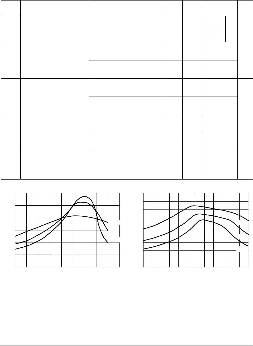
R
on
Maximum “ON” Resistance V
in
= V
IL
or V
IH
; V
IS
= V
CC
to
V
EE
; I
S
≤ 2.0 mA
(Figures 7, 8)
4.5
4.5
6.0
0.0
−4.5
−6.0
190
120
100
240
150
125
280
170
140
W
V
in
= V
IL
or V
IH
; V
IS
= V
CC
or
V
EE
(Endpoints); I
S
≤ 2.0 mA
(Figures 7, 8)
4.5
4.5
6.0
0.0
−4.5
−6.0
150
100
80
190
125
100
230
140
115
DR
on
Maximum Difference in “ON”
Resistance Between Any Two
Channels in the Same Package
V
in
= V
IL
or V
IH
;
V
IS
= 1/2 (V
CC
− V
EE
);
I
S
≤ 2.0 mA
4.5
4.5
6.0
0.0
−4.5
−6.0
30
12
10
35
15
12
40
18
14
W
I
off
Maximum Off−Channel Leakage
Current, Any One Channel
V
in
= V
IL
or V
IH
;
V
IO
= V
CC
− V
EE
;
Switch Off (Figure 9)
5.0 −5.0 0.1 0.5 1.0
mA
Maximum Off−Channel HCT4051A
Leakage Current, HCT4052A
Common Channel HCT4053A
V
in
= V
IL
or V
IH
;
V
IO
= V
CC
− V
EE
;
Switch Off (Figure 10)
5.0
5.0
5.0
−5.0
−5.0
−5.0
0.2
0.1
0.1
2.0
1.0
1.0
4.0
2.0
2.0
I
on
Maximum On−Channel HCT4051A
Leakage Current, HCT4052A
Channel−to−Channel HCT4053A
V
in
= V
IL
or V
IH
;
Switch−to−Switch =
V
CC
− V
EE
; (Figure 11)
5.0
5.0
5.0
−5.0
−5.0
−5.0
0.2
0.1
0.1
2.0
1.0
1.0
4.0
2.0
2.0
mA