LTC4444
6
4444fb
PIN FUNCTIONS
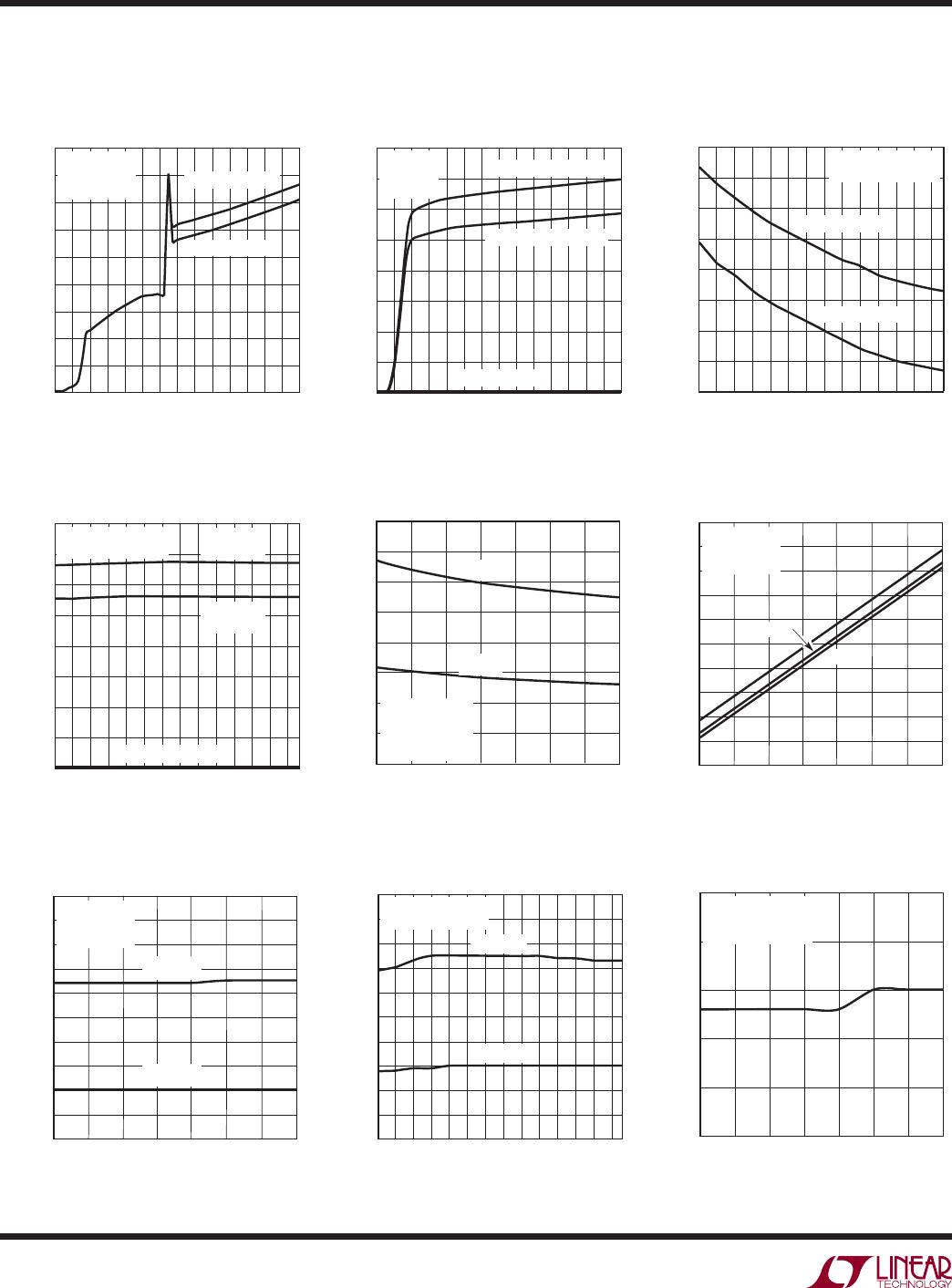
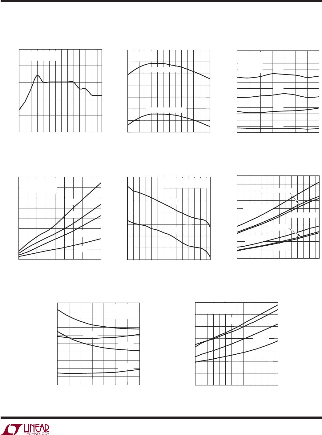
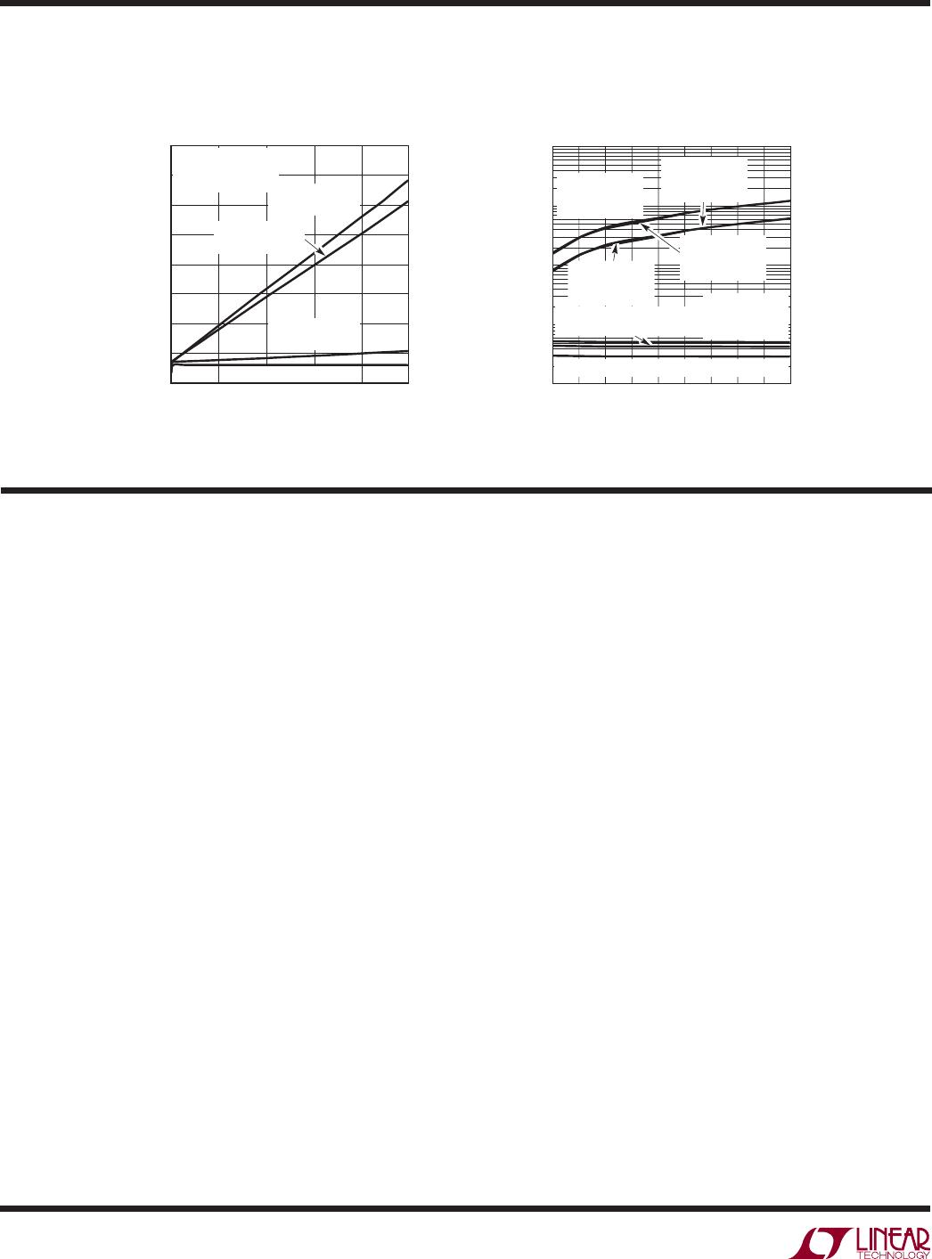
TYPICAL PERFORMANCE CHARACTERISTICS
Switching Supply Current
vs Input Frequency
Switching Supply Current
vs Load Capacitance
TINP (Pin 1): High Side Input Signal. Input referenced
to GND. This input controls the high side driver output
(TG).
BINP (Pin 2): Low Side Input Signal. This input controls
the low side driver output (BG).
V
CC
(Pin 3): Supply. This pin powers input buffers, logic
and the low side gate driver output directly and the high
side gate driver output through an external diode con-
nected between this pin and BOOST (Pin 6). A low ESR
ceramic bypass capacitor should be tied between this pin
and GND (Pin 9).
BG (Pin 4): Low Side Gate Driver Output (Bottom Gate).
This pin swings between V
CC
and GND.
NC (Pin 5): No Connect. No connection required.
BOOST (Pin 6): High Side Bootstrapped Supply. An ex-
ternal capacitor should be tied between this pin and TS
(Pin 8). Normally, a bootstrap diode is connected between
V
CC
(Pin 3) and this pin. Voltage swing at this pin is from
V
CC
– V
D
to V
IN
+ V
CC
– V
D
, where V
D
is the forward volt-
age drop of the bootstrap diode.
TG (Pin 7): High Side Gate Driver Output (Top Gate). This
pin swings between TS and BOOST.
TS (Pin 8): High Side MOSFET Source Connection (Top
Source).
GND (Exposed Pad Pin 9): Ground. Must be soldered to
PCB ground for optimal thermal performance.
SWITCHING FREQUENCY (kHz)
0
SUPPLY CURRENT (mA)
1.5
2.0
2.5
600
1000
4444 G18
1.0
0.5
0
200 400 800
3.0
3.5
4.0
I
BOOST
(TG SWITCHING)
I
BOOST
(BG SWITCHING)
I
VCC
(BG SWITCHING)
I
VCC
(TG SWITCHING)
T
A
= 25°C
V
CC
= BOOST = 12V
TS = GND
LOAD CAPACITANCE (nF)
1
SUPPLY CURRENT (mA)
10
100
1345
0.1
27896
10
4444 G19
I
VCC
(BG SWITCHING
AT 1MHz)
I
BOOST
(TG SWITCHING
AT 500kHz)
I
BOOST
(TG SWITCHING
AT 1MHz)
I
BOOST
(BG SWITCHING AT 1MHz OR 5OOkHz)
I
VCC
(BG SWITCHING
AT 500kHz)
I
VCC
(TG SWITCHING AT 500kHz)
I
VCC
(TG SWITCHING
AT 1MHz)