Expand menu
Hello, Sign in
My Account
0
Cart
Home
Products
Sensors
Semiconductors
Passive Components
Connectors
Power
Electromechanical
Optoelectronics
Circuit Protection
Integrated Circuits - ICs
Main Products
Manufacturers
Blog
Services
About OMO
About Us
Contact Us
Check Stock
IRF7101TRPBF
P1-P3
P4-P6
P7-P9
IRF7101PbF
C,
IRF7101PbF
10
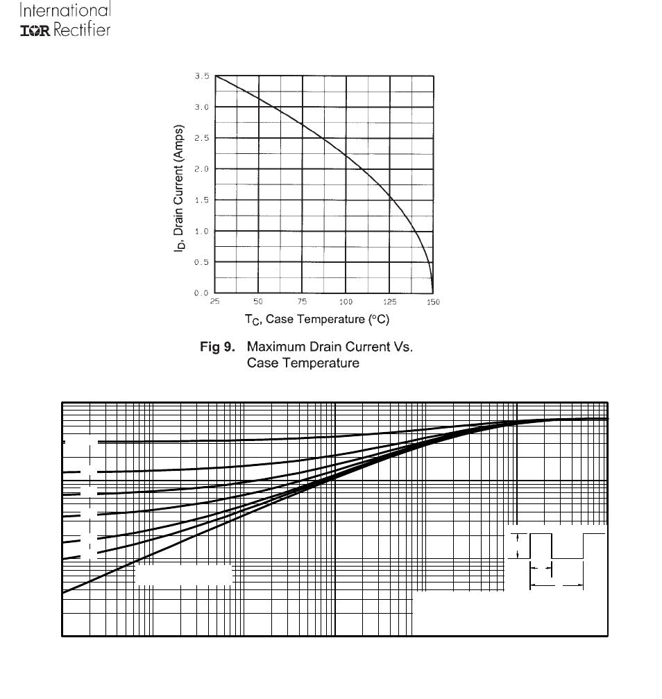
Fig 10.
Maximum Effective Transient
Thermal Impedance,
Junction-to-Ambient
0.1
1
10
100
0.0001
0.001
0.01
0.1
1
10
100
Notes:
1. D
uty
facto
r D =
t / t
2. Peak
T
=
P
x Z
+ T
1
2
J
DM
thJA
A
P
t
t
DM
1
2
t , R
ect
angul
a
r Pul
se
Durat
i
on (se
c
)
Thermal Response
(Z )
1
thJA
0.01
0.02
0.05
0.10
0.20
D = 0.
50
SINGLE PULSE
(
THER
MAL RESPONSE)
IRF7101PbF
Fig 12b.
Basic Gate Charge Waveform
Fig 12a.
Gate Charge
Test Circuit
D.U.T
.
V
DS
I
D
I
G
3mA
V
GS
.3
µ
F
50K
Ω
.2
µ
F
12V
Current
Regulator
Same
Type
as
D.U.T
.
Current
Sampling
Resistors
+
-
Q
G
Q
GS
Q
GD
V
G
Charge
10V
Fig 11a.
Switching Time Test
Circuit
+
-
V
DS
90%
10%
V
GS
t
d(on)
t
r
t
d(
off)
t
f
V
DS
10V
Pulse
Width
≤ 1
µs
Duty
Factor
≤
0.1
%
Fig 11b.
Switching Time Waveforms
R
D
V
GS
V
DD
R
G
D.U.T.
P1-P3
P4-P6
P7-P9
IRF7101TRPBF
Mfr. #:
Buy IRF7101TRPBF
Manufacturer:
Infineon / IR
Description:
MOSFET MOSFT DUAL NCh 20V 3.5A
Lifecycle:
New from this manufacturer.
Delivery:
DHL
FedEx
Ups
TNT
EMS
Payment:
T/T
Paypal
Visa
MoneyGram
Western
Union
Products related to this Datasheet
IRF7101TRPBF
IRF7101PBF