LTC2601/LTC2611/LTC2621
4
2601fb
SYMBOL PARAMETER CONDITIONS MIN TYP MAX UNITS
V
IL
Digital Input Low Voltage V
CC
= 4.5V to 5.5V
V
CC
= 2.5V to 5.5V
l
l
0.8
0.6
V
V
V
OH
Digital Output High Voltage Load Current = –100μA
l
V
CC
– 0.4 V
V
OL
Digital Output Low Voltage Load Current = +100μA
l
0.4 V
I
LK
Digital Input Leakage V
IN
= GND to V
CC
l
±1 μA
C
IN
Digital Input Capacitance (Note 4)
l
8pF
ELECTRICAL CHARACTERISTICS
The l denotes the specifi cations which apply over the full operating
temperature range, otherwise specifi cations are at T
A
= 25°C. REF = 4.096V (V
CC
= 5V), REF = 2.048V (V
CC
= 2.5V), V
OUT
unloaded,
unless otherwise noted. (Note 8)
The l denotes the specifi cations which apply over the full operating temperature range, otherwise specifi cations are at T
A
= 25°C.
REF = 4.096V (V
CC
= 5V), REF = 2.048V (V
CC
= 2.5V), V
OUT
unloaded, unless otherwise noted.
SYMBOL PARAMETER CONDITIONS
LTC2621/ LTC2621-1 LTC2611/ LTC2611-1 LTC2601/ LTC2601-1
UNITSMIN TYP MAX MIN TYP MAX MIN TYP MAX
AC Performance
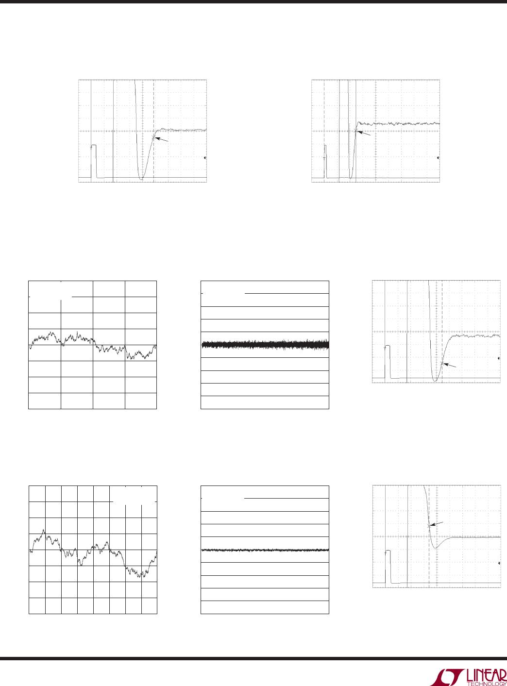
t
S
Settling Time (Note 6) ±0.024% (±1LSB at 12 Bits)
±0.006% (±1LSB at 14 Bits)
±0.0015% (±1LSB at 16 Bits)
77
9
7
9
10
μs
μs
μs
Settling Time for 1LSB Step
(Note 7)
±0.024% (±1LSB at 12 Bits)
±0.006% (±1LSB at 14 Bits)
±0.0015% (±1LSB at 16 Bits)
2.7 2.7
4.8
2.7
4.8
5.2
μs
μs
μs
Voltage Output Slew Rate 0.80 0.80 0.80 V/μs
Capacitive Load Driving 1000 1000 1000 pF
Glitch Impulse At Midscale Transition 12 12 12 nV • s
Multiplying Bandwidth 180 180 180 kHz
e
n
Output Voltage Noise
Density
At f = 1kHz
At f = 10kHz
120
100
120
100
120
100
nV/√Hz
nV/√Hz
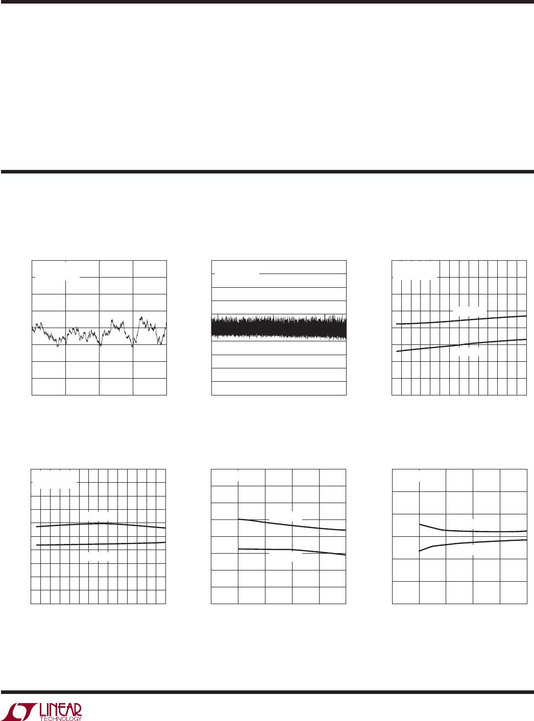
Output Voltage Noise 0.1Hz to 10Hz 15 15 15 μV
P-P
TIMING CHARACTERISTICS
The l denotes the specifi cations which apply over the full operating temperature
range, otherwise specifi cations are at T
A
= 25°C. (See Figure 1) (Notes 4, 8)
SYMBOL PARAMETER CONDITIONS MIN TYP MAX UNITS
V
CC
= 2.5V to 5.5V
t
1
SDI Valid to SCK Setup
l
4ns
t
2
SDI Valid to SCK Hold
l
4ns
t
3
SCK High Time
l
9ns
t
4
SCK Low Time
l
9ns
t
5
CS/LD Pulse Width
l
10 ns
t
6
LSB SCK High to CS/LD High
l
7ns
t
7
CS/LD Low to SCK High
l
7ns
t
8
SDO Propagation Delay from SCK Falling Edge C
LOAD
= 10pF
V
CC
= 4.5V to 5.5V
V
CC
= 2.5V to 5.5V
l
l
20
45
ns
ns
t
9
CLR Pulse Width
l
20 ns
t
10
CS/LD High to SCK Positive Edge
l
7ns
t
12
LDAC Pulse Width
l
15 ns
t
13
CS/LD High to LDAC High or Low Transition
l
200 ns
SCK Frequency 50% Duty Cycle
l
50 MHz