Data Sheet ADF4110/ADF4111/ADF4112/ADF4113
Rev. F | Page 13 of 28
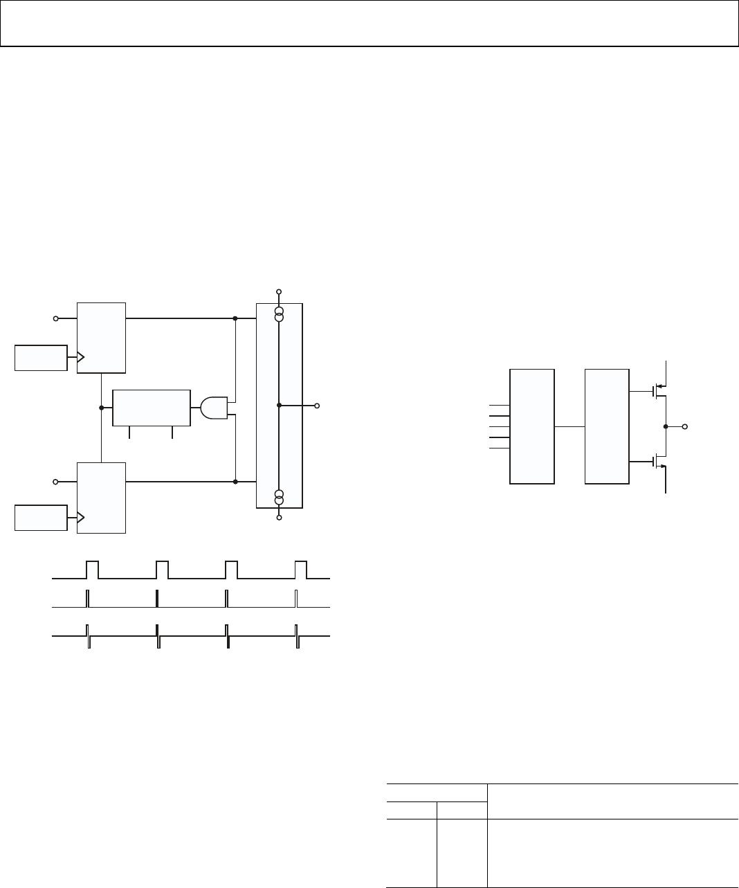
PHASE FREQUENCY DETECTOR (PFD) AND
CHARGE PUMP
The PFD takes inputs from the R counter and N counter (N =
BP + A) and produces an output proportional to the phase and
frequency difference between them. Figure 31 is a simplified
schematic. The PFD includes a programmable delay element
that controls the width of the antibacklash pulse. This pulse
ensures that there is no dead zone in the PFD transfer function
and minimizes phase noise and reference spurs. Two bits in the
reference counter latch, ABP2 and ABP1, control the width of
the pulse. See Table 7.
P
PROGRAMMABLE
DELAY
U3
CLR2
Q2D2
U2
CLR1
Q1D1
CHARGE
PUMP
DOWN
UP
HI
HI
U1
ABP1 ABP2
R DIVIDER
N DIVIDER
CP OUTPUT
R DIVIDER
N DIVIDER
CP
CPGND
V
03496-0-031
Figure 31. PFD Simplified Schematic and Timing (In Lock)
MUXOUT AND LOCK DETECT
The output multiplexer on the ADF4110 family allows the user
to access various internal points on the chip. The state of
MUXOUT is controlled by M3, M2, and M1 in the function
latch. Table 9 shows the full truth table. Figure 32 shows the
MUXOUT section in block diagram form.
Lock Detect
MUXOUT can be programmed for two types of lock detect:
digital lock detect and analog lock detect.
Digital lock detect is active high. When LDP in the R counter
latch is set to 0, digital lock detect is set high when the phase
error on three consecutive phase detector (PD) cycles is less
than 15 ns. With LDP set to 1, five consecutive cycles of less
than 15 ns are required to set the lock detect. It stays high until
a phase error greater than 25 ns is detected on any subsequent
PD cycle.
The N-channel open-drain analog lock detect should be
operated with a 10 kΩ nominal external pull-up resistor. When
lock has been detected, this output is high with narrow low-
going pulses.
CONTROLMUX
DV
DD
MUXOUT
DGND
ANALOG LOCK DETECT
DIGITAL LOCK DETECT
R COUNTER OUTPUT
N COUNTER OUTPUT
SDOUT
03496-0-032
Figure 32. MUXOUT Circuit
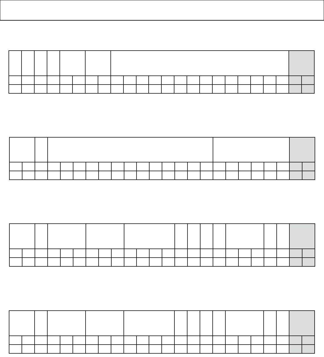
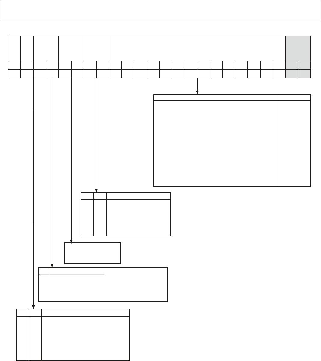
INPUT SHIFT REGISTER
The ADF4110 family digital section includes a 24-bit input shift
register, a 14-bit R counter, and a 19-bit N counter comprised of
a 6-bit A counter and a 13-bit B counter. Data is clocked into
the 24-bit shift register on each rising edge of CLK MSB first.
Data is transferred from the shift register to one of four latches
on the rising edge of LE. The destination latch is determined by
the state of the two control bits (C2, C1) in the shift register.
These are the two LSBs, DB1 and DB0, as shown in Figure 2.
The truth table for these bits is shown in Table 5.
Table 6 shows a summary of how the latches are programmed.
Table 5. C2, C1 Truth Table
Control Bits
C2 C1 Data Latch
0 0 R Counter
0 1 N Counter (A and B)
1 0 Function Latch (Including Prescaler)
1 1 Initialization Latch