X9314WSZ-3T1

4
FN8178.3
July 24, 2014
Submit Document Feedback
Absolute Maximum Ratings Recommended Operating Conditions
Temperature under bias. . . . . . . . . . . . . . . . . . . . . .-65C to +135C
Storage temperature . . . . . . . . . . . . . . . . . . . . . . . .-65°C to +150°C
Voltage on CS
, INC, U/D, and
V
CC
with respect to V
SS
. . . . . . . . . . . . . . . . . . . . . . . -1V to +7V
Voltage on V
H
/R
H
and V
L
/R
L
referenced
to V
SS
. . . . . . . . . . . . . . . . . . . . . . . . . . . . . . . . . . . . . . -8V to +8V
V = |V
H
/R
H
- V
L
/R
L
| . . . . . . . . . . . . . . . . . . . . . . . . . . . . . . . . .10V
Lead temperature (soldering 10s) . . . . . . . . . . . . . . . . . . . . .+300°C
Wiper current . . . . . . . . . . . . . . . . . . . . . . . . . . . . . . . . . . . . . . ±1mA
I
W
(10s) . . . . . . . . . . . . . . . . . . . . . . . . . . . . . . . . . . . . . . . . .±8.8mA
Temperature (Commercial) . . . . . . . . . . . . . . . . . . . . . 0°C to +70°C
Temperature (Industrial). . . . . . . . . . . . . . . . . . . . . . .-40°C to +85°C
Supply Voltage (V
CC
) Limits
X9314. . . . . . . . . . . . . . . . . . . . . . . . . . . . . . . . . . . . . . . 5V ± 10%
X9314-2.7. . . . . . . . . . . . . . . . . . . . . . . . . . . . . . . . . . . 3V to 5.5V
CAUTION: Do not operate at or near the maximum ratings listed for extended periods of time. Exposure to such conditions may adversely impact product reliability and
result in failures not covered by warranty.
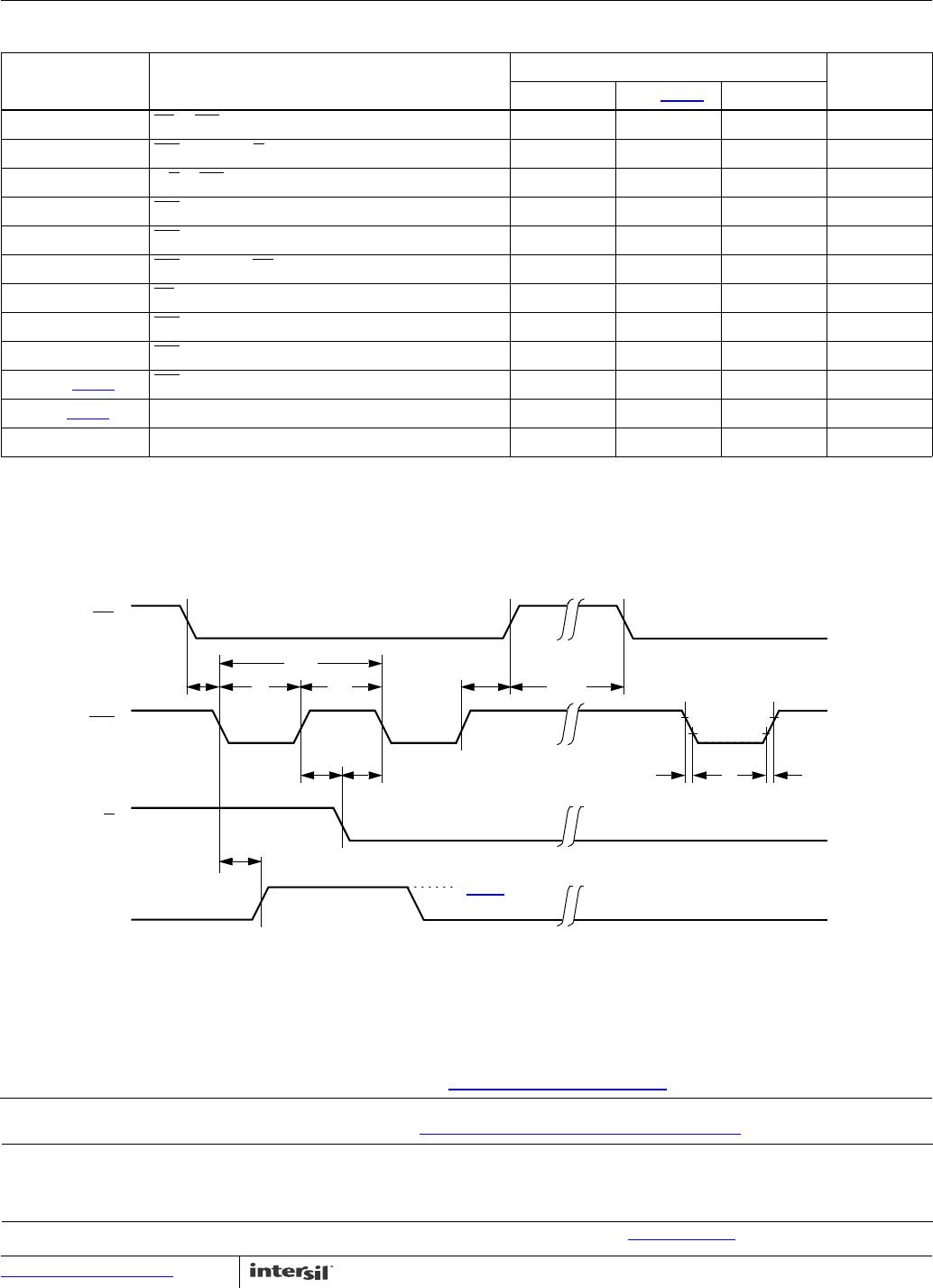
Potentiometer Characteristics Across recommended operating conditions unless otherwise specified.
SYMBOL PARAMETER TEST CONDITIONS/NOTES
LIMITS
MIN TYP MAX UNITS
R
TOTAL
End to End Resistance Tolerance ±20 %
V
H
/R
H
Terminal Voltage -5 +5 V
V
VL/RL
V
L
/R
L
Terminal Voltage -5 +5 V
Power Rating at +25°C 10 mW
R
W
Wiper Resistance I
W
= ±1mA, V
CC
= 5V 40 100
I
W
Wiper Current ±4.4 mA
Noise Ref: 1kHz -120 dBV
Relative variation. Error in step size
between taps.
log (R
w(n)
) - log R
w(n - 1)
) 0.07-
0.003
0.07 + 0.003
R
TOTAL
Temperature Coefficient for -40°C to +85°C ±600 ppm/°C
Ratiometric Temperature Coefficient ±20 ppm/°C
C
H
/C
L
/C
W
Note 4
Potentiometer Capacitance See Circuit #3 SPICE
Macromodel” on page 5
10/10/25 pF
X9314
5
FN8178.3
July 24, 2014
Submit Document Feedback
SYMBOL TABLE
DC Electrical Specifications Across recommended operating conditions unless otherwise specified.
SYMBOL PARAMETER TEST CONDITIONS
LIMITS
UNITSMIN
TYP
(Note 3
)MAX
I
CC
V
CC
Active Current CS = V
IL
, U/D = V
IL
or V
IH
and
INC
= 0.4V/2.4V at max. t
CYC
13mA
I
SB
Standby Supply Current CS = V
CC
- 0.3V, U/D and INC =V
SS
or
V
CC
- 0.3V
500 µA
I
LI
CS, INC, U/D Input Leakage Current V
IN
= V
SS
to V
CC
±10 µA
V
IH
CS, INC, U/D Input HIGH Voltage 2 V
CC
+ 1 V
V
IL
CS, INC, U/D Input LOW Voltage -1 0.8 V
C
IN
(Note 4)CS, INC, U/D Input Capacitance V
CC
= 5V, V
IN
= V
SS
, T
A
= +25°C, f = 1MHz 10 pF
NOTES:
3. Typical values are for T
A
= +25°C and nominal supply voltage.
4. This parameter is periodically sampled and not 100% tested.
Standard Parts
PART NUMBER MAXIMUM RESISTANCE WIPER INCREMENTS MINIMUM RESISTANCE
X9314W 10k Log Taper 40
Test Circuit #1 Test Circuit #2 Circuit #3 SPICE Macromodel
TEST POINT
V
W
/R
W
V
H
/R
H
V
L
/R
L
FORCE
CURRENT
V
W
/R
W
V
H
/R
H
V
L
/R
L
TEST POINT
10pF
R
H
R
TOTAL
C
H
25pF
C
W
C
L
10pF
R
W
R
L
MACRO MODEL
A.C. Conditions of Test
INPUT PULSE LEVELS 0V to 3V
Input rise and fall times 10ns
Input reference levels 1.5V
Mode Selection
CS INC U/D MODE
L H Wiper up
L L Wiper down
H X Store wiper position
H X X Standby
L X No store, return to standby
X9314
6
FN8178.3
July 24, 2014
Intersil products are manufactured, assembled and tested utilizing ISO9001 quality systems as noted
in the quality certifications found at www.intersil.com/en/support/qualandreliability.html
Intersil products are sold by description only. Intersil Corporation reserves the right to make changes in circuit design, software and/or specifications at any time
without notice. Accordingly, the reader is cautioned to verify that data sheets are current before placing orders. Information furnished by Intersil is believed to be
accurate and reliable. However, no responsibility is assumed by Intersil or its subsidiaries for its use; nor for any infringements of patents or other rights of third
parties which may result from its use. No license is granted by implication or otherwise under any patent or patent rights of Intersil or its subsidiaries.
For information regarding Intersil Corporation and its products, see www.intersil.com
For additional products, see www.intersil.com/en/products.html
Submit Document Feedback
A.C. Timing
NOTE:
7. MI in the A.C. timing diagram refers to the minimum incremental change in the V
W
output due to a change in the wiper position.
AC Electrical Specifications Across recommended operating conditions unless otherwise specified.
SYMBOL PARAMETER
LIMITS
UNITSMIN TYP(Note 5
)MAX
t
Cl
CS to INC Setup 100 ns
t
lD
INC HIGH to U/D Change 100 ns
t
DI
U/D to INC Setup 2.9 µs
t
lL
INC LOW Period 1 µs
t
lH
INC HIGH Period 1 µs
t
lC
INC Inactive to CS Inactive 1 µs
t
CPH
CS Deselect Time 20 ms
t
IW
INC to V
W
Change 100 500 µs
t
CYC
INC Cycle Time 4 µs
t
R
, t
F
(Note 6)INC Input Rise and Fall Time 500 µs
t
PU
(Note 6)
Power-up to Wiper Stable 500 µs
t
R
V
CC
V
CC
Power-up Rate 0.2 50 mV/µs
NOTES:
5. Typical values are for T
A
= +25°C and nominal supply voltage.
6. This parameter is periodically sampled and not 100% tested.
CS
INC
U/D
V
W
t
CI
t
IH
t
CYC
t
ID
t
DI
t
IW
MI
t
IC
t
CPH
t
F
t
R
10%
90% 90%
t
IL
Note 7
X9314

X9314WSZ-3T1

Mfr. #:
Manufacturer:
Renesas / Intersil
Description:
Digital Potentiometer ICs 10KOHM LOG TAPER CMOS EEPOT 8LD COM
Lifecycle:
New from this manufacturer.
Delivery:
DHL FedEx Ups TNT EMS
Payment:
T/T Paypal Visa MoneyGram Western Union