LTC2921/LTC2922 Series
12
29212fa
voltage specifications. On-resistance is a critical param-
eter when choosing power MOSFETs. The integrated
remote sense switches compensate for IR drops, but
minimizing V
Q(MAX)
leaves more margin for designing the
resistive voltage divider for the monitors.
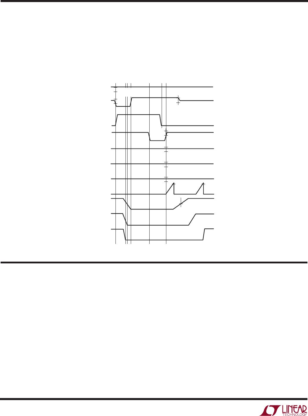
Setting the GATE Ramp Rate
Application of power to the loads is controlled by setting
the voltage ramping rate with an external capacitor on the
GATE pin. During Step 3 of the monitoring sequence, a
10µA pull-up ramps the GATE pin capacitance up to
V
PUMP
, the internal charge pump voltage. Use Equation 5
to calculate the nominal GATE pin capacitance necessary
to achieve a given ramp rate, ∆V/∆t:
C
A
Vt
GATE
=
µ
∆∆
10
/
(5)
Alternatively, to calculate the GATE capacitor to achieve a
desired nominal ramp time, use Equation 6. The GATE
drive voltage (V
GATE
) varies with V
CC
voltage. Consult the
Electrical Characteristics table and Typical Performance
curves to choose an appropriate value to insert for V
GATE
.
C
At
V
GATE
RAMP
GATE
=
µ10 •
(6)
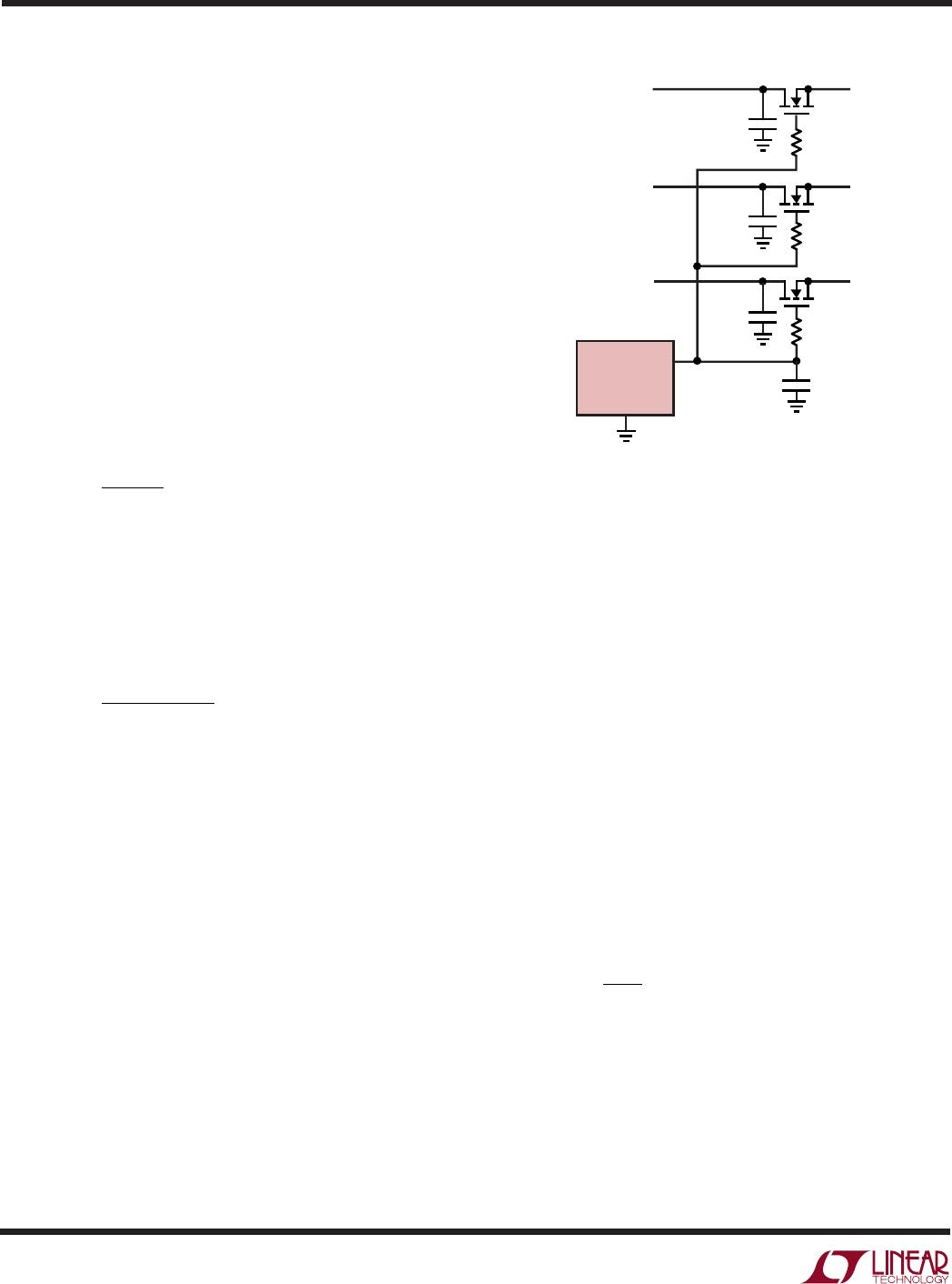
When the GATE pin drives several FETs in parallel, the load
voltages ramp together at the same rate until the lowest
supply reaches its full value. The other supplies continue
to track until the next lowest supply reaches its full value,
and so on.
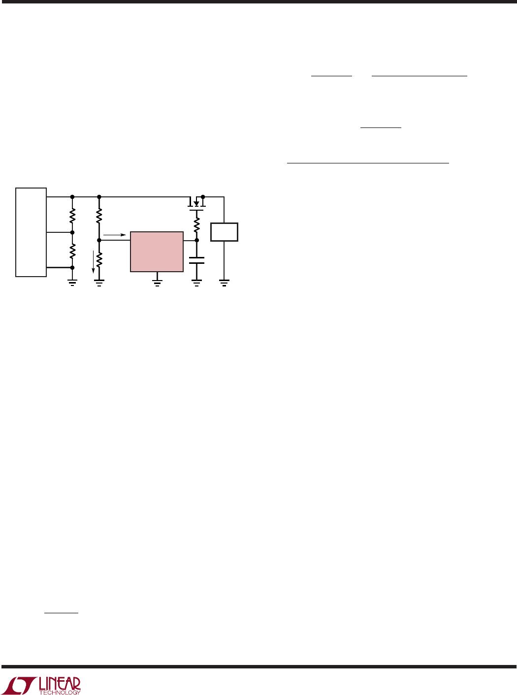
The GATE pin must not be forced above the level it reaches
when fully ramped. An internal clamp limits the GATE
voltage to ≤12.2V relative to ground.
Damp possible ramp-on oscillations by including a 10Ω
resistor in series with each external N-channel gate, and as
necessary, a 0.1µF capacitor on each external N-channel
drain, as shown in Figure 6.
Setting the Sequence Delay Timer
The turn-on sequence includes two programmable delays
set by the capacitance on the TIMER pin. More precisely,
a single delay value is used at two points in the sequence.
APPLICATIO S I FOR ATIO
WUUU
In both cases, the delay provides a measure of confidence
that conditions are stable enough for the sequence to
advance.
The first TIMER delay begins once all monitor voltages
comply with their thresholds, the electronic circuit breaker
has not tripped, and V
CC
is not undervoltage. The TIMER
pin sources 2µA into an external capacitor, which ramps
its voltage. A comparator trips when the TIMER pin voltage
reaches the internal 1.2V reference, then the GATE ramp
begins, and TIMER is pulled to ground. The second TIMER
delay begins after the gate of the remote sense switches is
fully ramped up. After the TIMER ramp completes, the PG
pin is activated. An internal circuit pulls-down the TIMER
pin with >100µA of current at all times, except during the
ramping periods, and when V
CC
is undervoltage.
Calculate the nominal value for the timing capacitor by
inserting the desired delay into Equation 7:
C
A
V
t
TIMER DLY
=
µ2
12.
•
(7)
For delay times below 60µs, be sure to limit stray capaci-
tances on the TIMER pin by using good PCB design
practices. To program essentially no delay (<1µs), float
the TIMER pin.
Internal circuitry guarantees that the TIMER pin is pulled
below 150mV (typical) before a delay cycle can begin.
LTC2922
GND
GATE
R
G2
10Ω
R
G1
10Ω
R
G0
10Ω
Q2
Q1
Q0
C
GATE
C
D2
0.1µF
(OPT)
C
D1
0.1µF
(OPT)
C
D0
0.1µF
(OPT)
V
SRC2
V
SRC1
V
SRC0
2921/22 F06
V
L2
V
L1
V
L0
Figure 6. Ramping and Damping Components on GATE Pin