LTC2921/LTC2922 Series
17
29212fa
APPLICATIO S I FOR ATIO
WUUU
Next, consider the supply ramping N-channel MOSFETs
Q0, Q1 and Q2. Transistor Q0 will have >4.5V of gate-
source voltage, even at maximum supply voltage (5.375V)
and minimum GATE pin voltage (10V). Considering the
voltages, temperatures, and currents involved, the maxi-
mum on-resistance (R
Q(ON)(MAX)
) of the Vishay Siliconix
Si2316DS is about 150mΩ. Switches Q1 and Q2 will see
even higher gate-source voltages, implying even smaller
R
Q(ON)(MAX)
values. Table 2 summarizes the calculated
V
Q(ON)(MAX)
voltages. Include the additional 50mV drop
across R
SENSE
when budgeting for the V
CC
supply path.
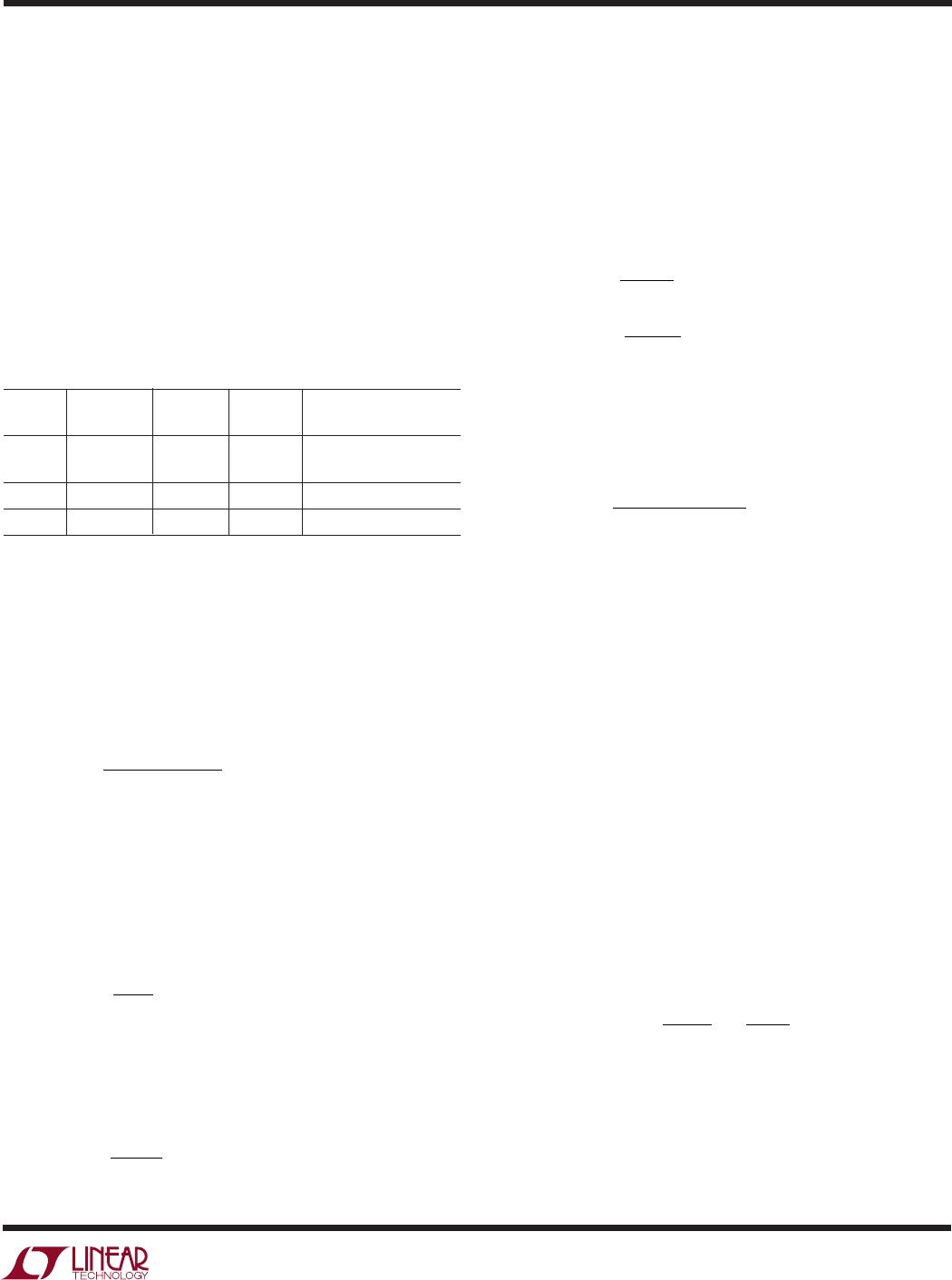
Table 2. External MOSFET Drain-Source Voltage Drops
Supply External R
Q(ON)
I
L
V
Q(ON)
Voltage MOSFET Max Max Max
120mV
5V Q0 ~150mΩ 0.8A (+50mV = 170mV)
3.3V Q1 <150mΩ 1.6A <240mV
2.5V Q2 <150mΩ 0.4A <60mV
The ±20V absolute maximum gate-source voltage rating
of the Si2316DS easily accommodates this design.
Next, calculate the necessary capacitance on the GATE pin
to realize the desired ramp rate. Use the nominal value of
V
GATE
from the Electrical Specification, and choose a
standard value.
C
Ams
V
FF
GATE
=
µ
=µ≈µ
10 500
10 8
0 463 0 47
•
.
..
Include drain bypass capacitors of 0.1µF and series gate
resistors of 10Ω on each external power FET to damp turn-
on oscillations.
Find the capacitance at the TIMER pin required to set the
delays in the power-on sequence:
C
A
V
ms F F
TIMER
=
µ
=µ≈µ
2
12
150 0 25 0 22
.
•..
The application requires the use of the circuit breaker
function on the V
CC
supply. First, find the upper limit on the
sense resistor value:
R
mV
A
m
SENSE
≤= Ω
45
08
53 25
.
.
Select a precision power sense resistor, such as the
Vishay Dale WSL1206 series. They can be specified to 1%,
and exhibit <1% variation over the LTC2921/LTC2922
operating range; choose R
SENSE
= 50mΩ. Including toler-
ances, the circuit breaker trip current threshold variation
will be:
I
mV
m
A
I
mV
m
A
TRIP MIN
TRIP MAX
()
()
.
.
=
Ω
=
=
Ω
=
45
51
088
55
49
112
The PG pin is configured as a 2.5V negative-logic reset
signal for the microcontroller. The minimum pull-up resis-
tance for proper operation is:
R
VV
mA
PG MIN()
.–.
=≈Ω
2 6875 0 4
5
460
Figure 13 shows R
PG
= 4.7k. The value is somewhat
arbitrarily chosen, but it does limit the pull-down current
to <500µA. Trade off lower pull-down currents against
faster pull-up edge rates in other applications.
Recall that proper operation of the remote load sensing
function requires:
R
Q(ON)
, R
FB(ON)
<< R
X
<< (R
Y
+R
Z
)
In this example, the operating conditions and the Si2316DS
give R
Q(ON)(MAX)
= 150mΩ, the Electrical Characteristics
table guarantees R
FB(ON)
< 10Ω, and the example design
specification requires that (R
Y
+ R
Z
) <100k. Selecting R
X0
= R
X1
= R
X2
= 100Ω satisfies the inequality.
Before the loads are connected to the supplies, the voltage
error due to the R
X
resistors will be <0.1% for all three
supplies:
∆=
Ω
==VV
k
V
of V
SRC SRC
SRC
SRC
•.%
100
100 1000
01
After the remote sense switches close, the load voltage
errors due to R
X
at maximum loads will be:

