Nexperia
HEF4047B
Monostable/astable multivibrator
HEF4047B All information provided in this document is subject to legal disclaimers. © Nexperia B.V. 2017. All rights reserved.
Product data sheet Rev. 6 — 17 March 2017
7 / 22
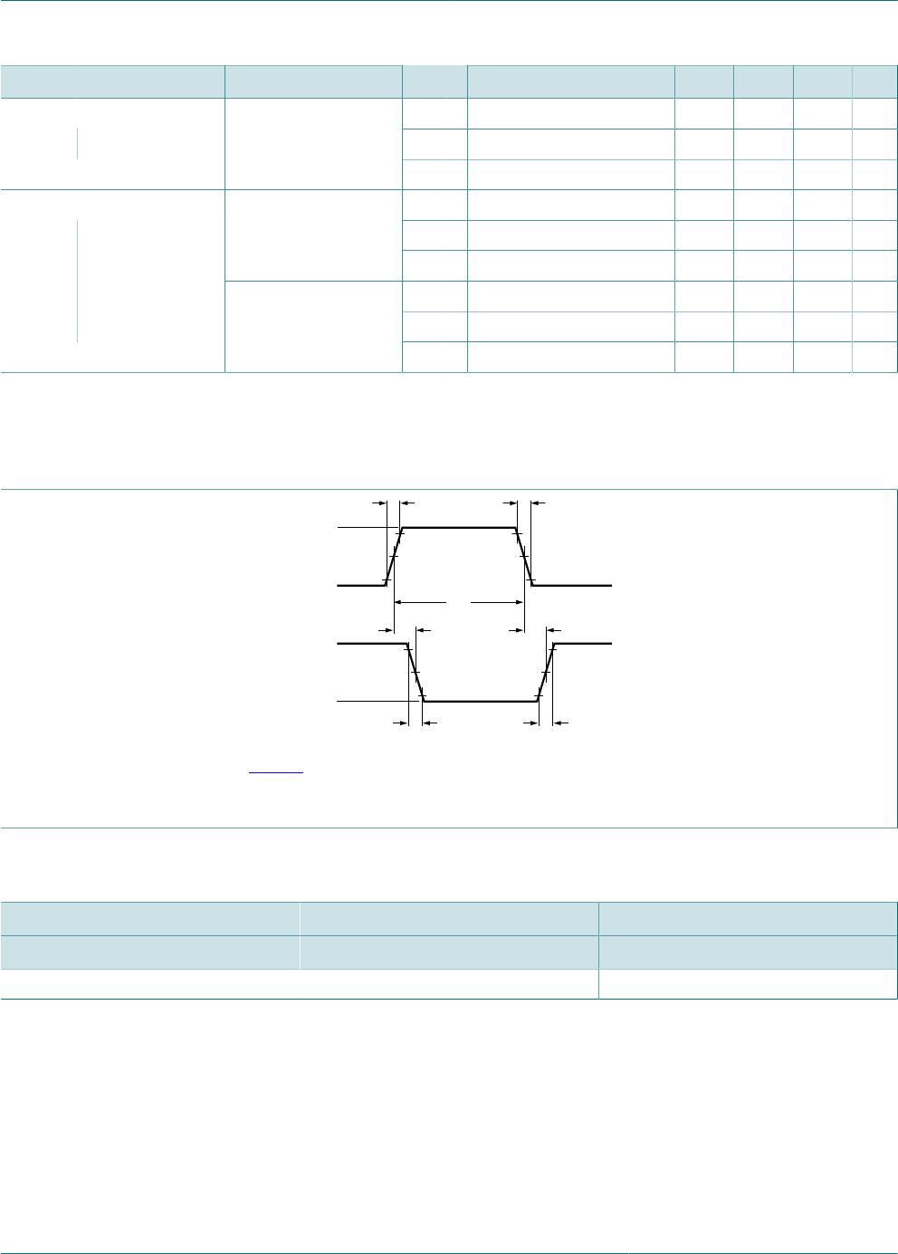
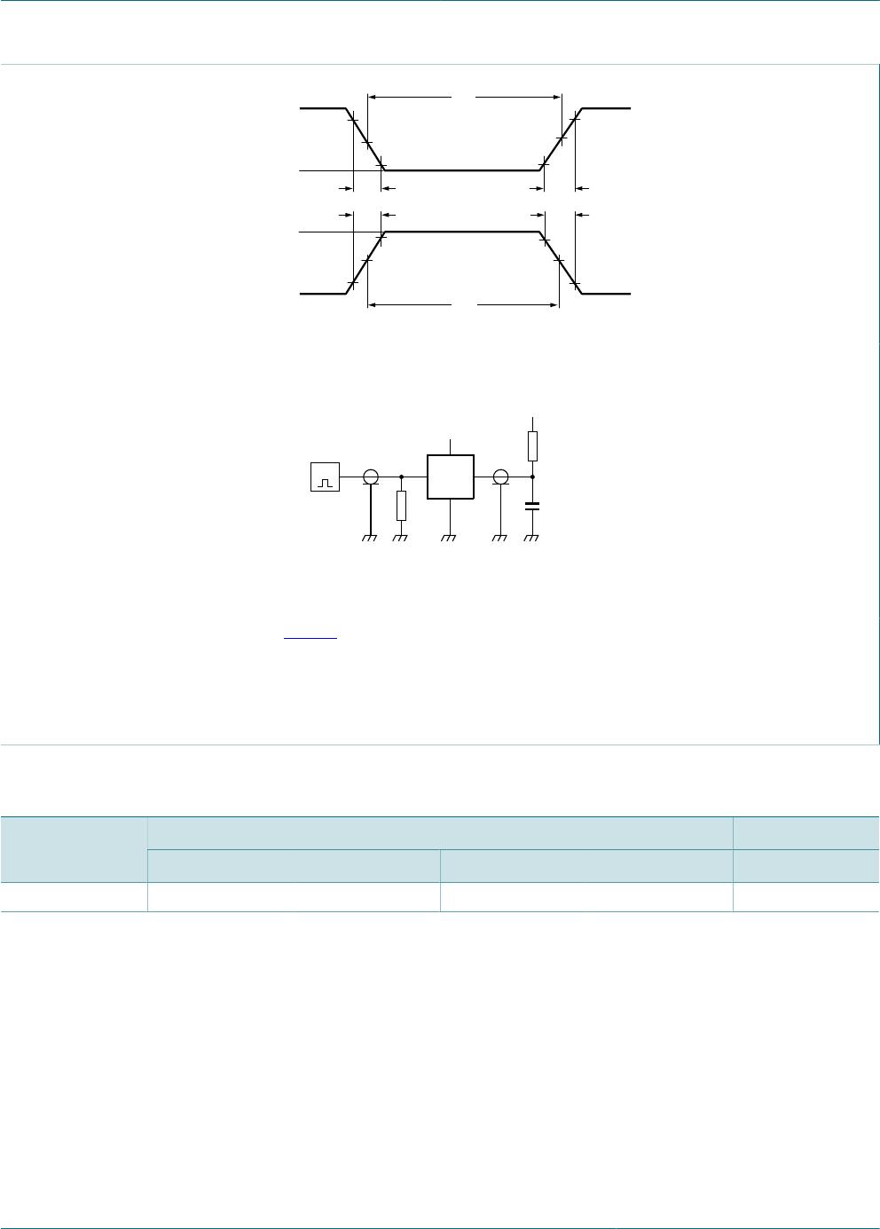
10 Dynamic characteristics
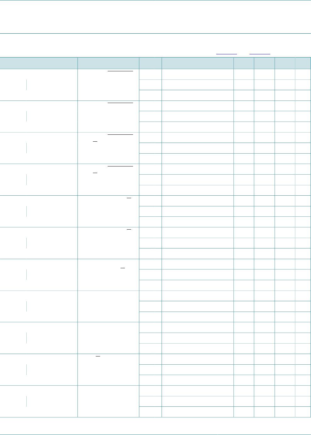
Table 6. Dynamic characteristics
V
SS
= 0 V; T
amb
= 25 °C; unless otherwise specified; for waveform and test circuit, see Figure 4 and Figure 5.
Symbol Parameter Conditions V
DD
Extrapolation formula Min Typ Max Unit
5 V
[1]
68 ns + (0.55 ns/pF)C
L
- 95 190 ns
10 V
[1]
43 ns + (0.23 ns/pF)C
L
- 45 90 ns
t
PHL
HIGH to LOW
propagation delay
ASTABLE, ASTABLE
to OSCILLATOR
OUTPUT
15 V
[1]
22 ns + (0.16 ns/pF)C
L
- 30 60 ns
5 V
[1]
58 ns + (0.55 ns/pF)C
L
- 85 170 ns
10 V 29 ns + (0.23 ns/pF)C
L
- 40 80 ns
t
PLH
LOW to HIGH
propagation delay
ASTABLE, ASTABLE
to OSCILLATOR
OUTPUT
15 V 22 ns + (0.16 ns/pF)C
L
- 30 60 ns
5 V
[1]
123 ns + (0.55 ns/pF)C
L
- 150 300 ns
10 V 54 ns + (0.23 ns/pF)C
L
- 65 130 ns
t
PHL
HIGH to LOW
propagation delay
ASTABLE, ASTABLE
to O, O
15 V 42 ns + (0.16 ns/pF)C
L
- 50 100 ns
5 V
[1]
103 ns + (0.55 ns/pF)C
L
- 130 260 ns
10 V 49 ns + (0.23 ns/pF)C
L
- 60 120 ns
t
PLH
LOW to HIGH
propagation delay
ASTABLE, ASTABLE
to O, O
15 V 37 ns + (0.16 ns/pF)C
L
- 45 90 ns
5 V
[1]
133 ns + (0.55 ns/pF)C
L
- 160 320 ns
10 V 54 ns + (0.23 ns/pF)C
L
- 65 130 ns
t
PHL
HIGH to LOW
propagation delay
+/-TRIGGER to O, O
15 V 42 ns + (0.16 ns/pF)C
L
- 50 100 ns
5 V
[1]
128 ns + (0.55 ns/pF)C
L
- 155 310 ns
10 V 54 ns + (0.23 ns/pF)C
L
- 65 130 ns
t
PLH
LOW to HIGH
propagation delay
+/-TRIGGER to O, O
15 V 42 ns + (0.16 ns/pF)C
L
- 50 100 ns
5 V
[1]
38 ns + (0.55 ns/pF)C
L
- 65 130 ns
10 V 19 ns + (0.23 ns/pF)C
L
- 30 60 ns
t
PHL
HIGH to LOW
propagation delay
+TRIGGER,
RETRIGGER to O
15 V 17 ns + (0.16 ns/pF)C
L
- 25 50 ns
5 V
[1]
68 ns + (0.55 ns/pF)C
L
- 95 190 ns
10 V 29 ns + (0.23 ns/pF)C
L
- 40 80 ns
t
PLH
LOW to HIGH
propagation delay
+TRIGGER,
RETRIGGER to O
15 V 22 ns + (0.16 ns/pF)C
L
- 30 60 ns
5 V
[1]
83 ns + (0.55 ns/pF)C
L
- 100 200 ns
10 V 34 ns + (0.23 ns/pF)C
L
- 45 90 ns
t
PHL
HIGH to LOW
propagation delay
MR to O
15 V 27 ns + (0.16 ns/pF)C
L
- 35 70 ns
5 V
[1]
83 ns + (0.55 ns/pF)C
L
- 100 200 ns
10 V 34 ns + (0.23 ns/pF)C
L
- 45 90 ns
t
PLH
LOW to HIGH
propagation delay
MR to O
15 V 27 ns + (0.16 ns/pF)C
L
- 35 70 ns
5 V
[1]
10 ns + (1.0 ns/pF)C
L
- 60 120 ns
10 V 9 ns + (0.42 ns/pF)C
L
- 30 60 ns
t
THL
HIGH to LOW
output transition
time
15 V 6 ns + (0.28 ns/pF)C
L
- 20 40 ns