VS-VSK.166..PbF, VS-VSK.196..PbF, VS-VSK.236..PbF Series
www.vishay.com
Vishay Semiconductors
Revision: 29-Sep-15
4
Document Number: 94357
For technical questions within your region: DiodesAmericas@vishay.com
, DiodesAsia@vishay.com, DiodesEurope@vishay.com
THIS DOCUMENT IS SUBJECT TO CHANGE WITHOUT NOTICE. THE PRODUCTS DESCRIBED HEREIN AND THIS DOCUMENT
ARE SUBJECT TO SPECIFIC DISCLAIMERS, SET FORTH AT www.vishay.com/doc?91000
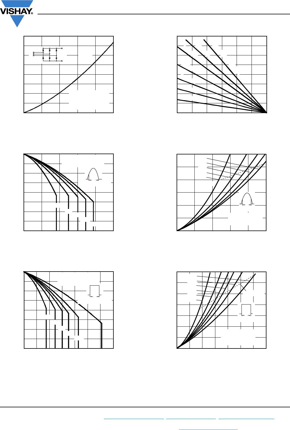
Fig. 5 - Maximum Non-Repetitive Surge Current Fig. 6 - Maximum Non-Repetitive Surge Current
Fig. 7 - On-State Power Loss Characteristics
Fig. 8 - On-State Power Loss Characteristics
2500
2000
1500
1000
4000
3500
3000
Peak Half Sine Wave
Forward Current (A)
Number of Equal Amplitude Half
Cycle Current Pulses (N)
10 1001
at 60 Hz 0.0083 s
at 50 Hz 0.0100 s
At any rated load condition and with
rated V
RRM
applied following surge.
VSK.166.. Series
Initial T
J
= 150 °C
500
4000
3500
3000
2500
2000
1500
1000
Peak Half Sine Wave
Forward Current (A)
Pulse Train Duration (s)
0.1
1
0.01
Maximum non-repetitive surge current
Initial T
J
= 150 °C
No voltage reapplied
Rated V
RRM
reapplied
versus pulse train duration.
VSK.166.. Series
0
100
150
200
250
300
50
Maximum Total Forward
Power Loss (W)
Total RMS Output Current (A)
50 100 150 200
250
0
DC
VSK.166.. Series
Per junction
T
J
= 150 °C
0
200
250
300
150
100
50
Maximum Total Forward
Power Loss (W)
Maximum Allowable Ambient Temperature (°C)
25 50 75 100 125
150
0
R
thSA
= 0.12 K/W - ΔR
0.2 K/W
0.3 K/W
0.4 K/W
0.5 K/W
0.7 K/W
0
1200
1800
Maximum Total Power Loss (W)
Total Output Current (A)
0
180°
(Sine)
180°
(Rect)
2 x VSK.166.. Series
Single phase bridge
Connected
T
J
= 150 °C
+
-
~
1600
1400
1000
800
600
400
200
100
200
300
400
500
0
800
600
400
200
1800
1600
1400
1200
1000
Maximum Total Power Loss (W)
Maximum Allowable Ambient Temperature (°C)
25 50 75 100 125
150
0
R
thSA
= 0.12 K/W - ΔR
0.04 K/W
0.06 K/W
0.1 K/W
0.16 K/W
0.25 K/W
0.5 K/W