Expand menu
Hello, Sign in
My Account
0
Cart
Home
Products
Sensors
Semiconductors
Passive Components
Connectors
Power
Electromechanical
Optoelectronics
Circuit Protection
Integrated Circuits - ICs
Main Products
Manufacturers
Blog
Services
About OMO
About Us
Contact Us
Check Stock
MC33341D
P1-P3
P4-P6
P7-P9
P10-P12
P13-P15
P16-P18
P19-P19
MC33341
http://onsemi.com
13
R3
Load
R1
Battery or
Resistive
Load
Source
Return
Source
R2
R
S
Comp
The above figure shows the MC33341 configured for load low−side current sensing allowing common paths for both power and ground
,
between the source and load. The Noninverting input paths, Pins 1 and 4, are used to sense the load induced voltage drop that a
ppear
s
across
resistor R
S
. The internal voltage and current regulation thresholds are selected by the respective external connections of Pins 2 an
d
6. Resistor R3 is required in applications where high peak levels of load current are possible from the battery or load bypass
capacitor
. Th
e
resistor value should be chosen to limit the negative substratecurrent to less than 20 mA. Excessively large values for R3 will
degrade th
e
current sensing accuracy
.
V
reg
+
V
th
(V)
ǒ
R2
R1
)
1
Ǔ
+
1.2
ǒ
R2
R1
)
1
Ǔ
I
reg
+
V
th
(ILS
)
)
R
S
+
0.2
R
S
R3
+
ǒ
I
pk
R
S
Ǔ
–0.6
0.02
V
I
Load
87
6
5
12
3
4
R
R
R
R
R
V
CC
V
CC
V
CC
V
CC
V
CC
V
CC
0.4 V
1.2 V
R
0.2 V
V
CC
0.2 V
0.4 V
1.2 V
V
CC
1.2 V
V
CC
Inverting Amp
Transconductance
Amp
Differential Amp
Disable Logic
Differential Amp
Opto
Isolator
V
sen
V
th
I
sen
I
th
Reference
Figure 20. Load Low−Side Current Sensing with
Internally Fixed Current and V
oltage Thresholds
MC33341
http://onsemi.com
14
R3
Load
R1
Battery or
Resistive
Load
Source
Return
Source
R2
R
S
Comp
The above figure shows the MC33341 configured for load low−side current sensing with an externally adjustable voltage and curre
n
t
threshold. Operation of this circuit is similar to that of Figure 20. The respective voltage and current regulation threshold c
an be adjusted
over a range of 0 to 1.2 V and 0 V to 200 mV
, with respect to Pin 4.
V
I
Load
87
6
5
12
3
4
R
R
R
R
R
V
CC
V
CC
V
CC
V
CC
V
CC
V
CC
0.4 V
1.2 V
R
0.2 V
V
CC
0.2 V
0.4 V
1.2 V
V
CC
1.2 V
V
CC
Inverting Amp
Transconductance
Amp
Differential Amp
Disable Logic
Differential Amp
Opto
Isolator
V
sen
V
th
I
sen
I
th
Reference
Figure 21. Load Low−Side Current Sensing with
Externally Adjustable Current and V
oltage Thresholds
V
reg
+
V
th
(Pin6)
ǒ
R2
R1
)
1
Ǔ
I
reg
+
V
th
(Pin2)
R
S
R3
+
ǒ
I
pk
R
S
Ǔ
–0.6
0.02
Current
Control
V
oltage
Current
MC33341
http://onsemi.com
15
Load
Source
Source
Load
1
87
6
5
234
MC33341
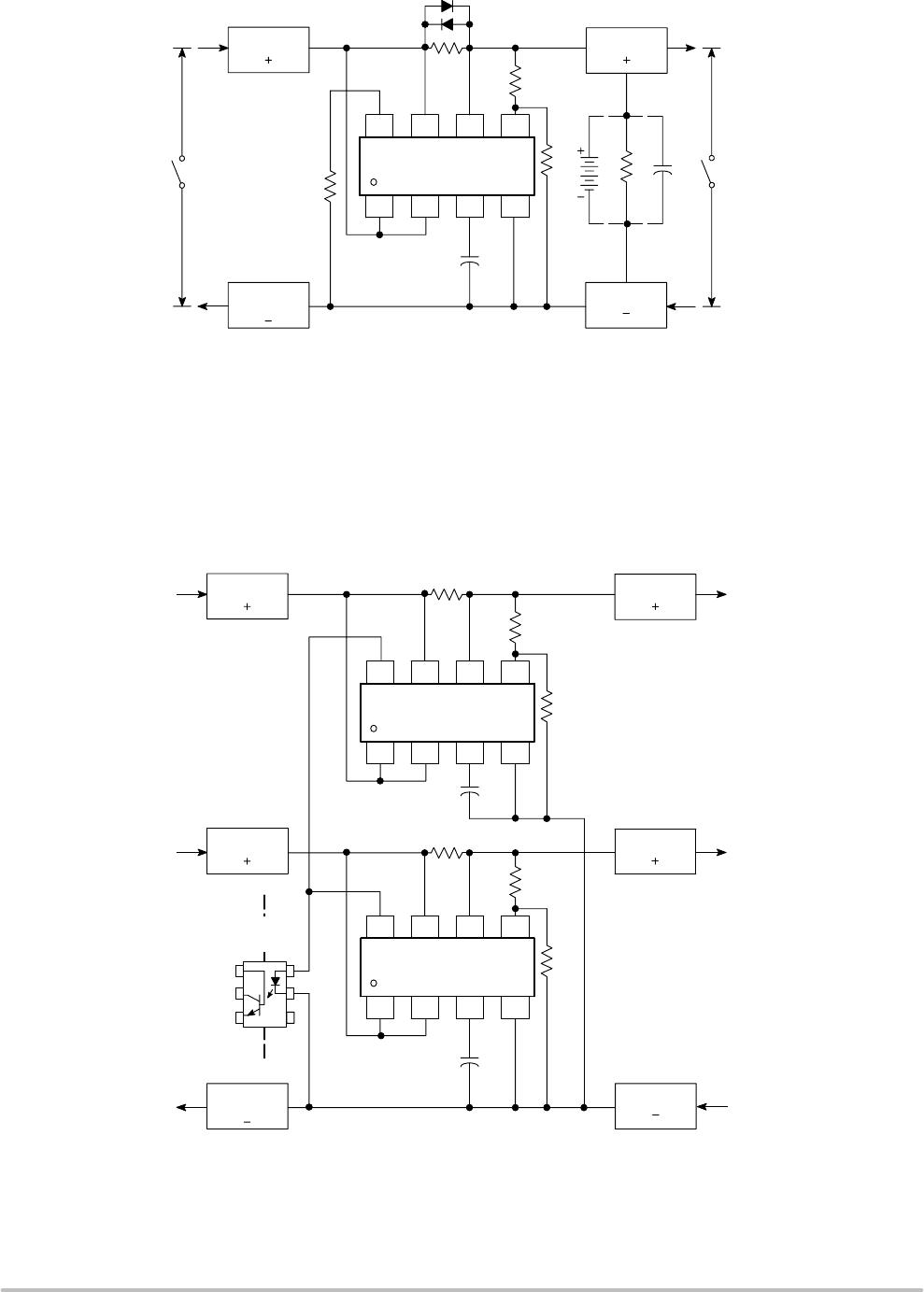
Figure 22. Current Sense Resistor Bounding
Figure 23. Multiple Output Current and V
oltage Regulation
Source
Source
Return
Load
Load
Output
Short
1
8765
234
Input
Short
R
S
MC33341
NOTE:
An excessive load induced voltage across R
S
can occur if either the source input or load output is shorted. This voltage can
easily be bounded with the addition of the diodes shown without degrading the current sensing accuracy
. This bounding technique
can be used in any of the MC33341 applications where high peak currents are anticipated.
NOTE:
Multiple outputs can be controlled by summing the error signal into a common optoisolator
. The converter output with the l
argest
voltage or current error will dominate control of the feedback loop.
Source
Return
Load
1
876
5
234
MC33341
Output 2
Output 1
Output Common
Opto
Isolator
P1-P3
P4-P6
P7-P9
P10-P12
P13-P15
P16-P18
P19-P19
MC33341D
Mfr. #:
Buy MC33341D
Manufacturer:
ON Semiconductor
Description:
Battery Management 2.3-15V Power Supply
Lifecycle:
New from this manufacturer.
Delivery:
DHL
FedEx
Ups
TNT
EMS
Payment:
T/T
Paypal
Visa
MoneyGram
Western
Union
Products related to this Datasheet
MC33341D
MC33341DR2
MC33341PG
MC33341DG
MC33341DR2G
MC33341P