SMCJ Transient Voltage Suppressor Diode Series
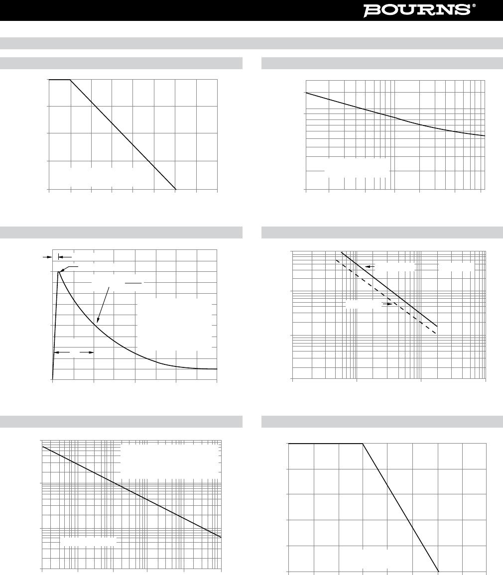
Rating & Characteristic Curves
Pulse Derating Curve Maximum Non-Repetitive Surge Current
Pulse Waveform Typical Junction Capacitance
Pulse Rating Curve Steady State Power Derating Curve
75
50
25
0
050
25 75 100 150125 175 200
Ambient Temperature (
Peak Pulse Derating in Percent of
Peak Power or Current
°C)
10 x 1000 Waveform as Defined
by R.E.A.
5.0
3.0
4.0
2.0
1.0
0.0
05025 75 100 150125 175 200
TL, Lead Temperature (°C)
RM(AV) Steady State Power Dissipation (W)
60 Hz Resistive or
Inductive Load
100
50
0
0 1.0 2.0 3.0 4.0
T, Time (ms)
I
P
, Peak Pulse Current (%)
TA=25 °C
TP
TR=10 µs
Half value=
IRSM
2
Peak value (IRSM)
Pulse width (TP)
is defined as that point
where the peak current
decays to 50 % of IPSM.
10 x 1000 waveform
as defined by R.E.A.
Peak Forward Surge Current (Amps)
100
200
10
1
2510 20 50 100
Number of Cycles at 60 Hz
Pulse Width 8.3 ms
Single Half Sine-Wave
(JEDEC Method)
Capacitance (pF)
10000
100
0
0
10 100 1000
Standoff Voltage (Volts)
1000
Bidirectional
TA = 25 °C
Unidirectional
100
1.0
10
0.1
0.1 µs
1.0 µs 10 µs 100 µs 1.0 ms 10 ms
TP, Pulse Width
P
P
, Peak Power (KW)
TA = 25 °C
Non-repetitive Pulse Waveform
Shown in Pulse Waveform Graph
8.0 mm Lead Areas
100
75
50
25
0
05025 75 100 150125 175 200
Ambient Temperature (
Peak Pulse Derating in Percent of
Peak Power or Current
°C)
10 x 1000 Waveform as Defined
by R.E.A.
5.0
3.0
4.0
2.0
1.0
0.0
05025 75 100 150125 175 200
TL, Lead Temperature (°C)
RM(AV) Steady State Power Dissipation (W)
60 Hz Resistive or
Inductive Load
100
50
0
0 1.0 2.0 3.0 4.0
T, Time (ms)
I
P
, Peak Pulse Current (%)
TA=25 °C
TP
TR=10 µs
Half value=
IRSM
2
Peak value (IRSM)
Pulse width (TP)
is defined as that point
where the peak current
decays to 50 % of IPSM.
10 x 1000 waveform
as defined by R.E.A.
Peak Forward Surge Current (Amps)
100
200
10
1
2510 20 50 100
Number of Cycles at 60 Hz
Pulse Width 8.3 ms
Single Half Sine-Wave
Capacitance (pF)
10000
100
0
0
10 100 1000
Standoff Voltage (Volts)
1000
Bidirectional
TA = 25 °C
Unidirectional
100
1.0
10
0.1
0.1 µs
1.0 µs 10 µs 100 µs 1.0 ms 10 ms
TP, Pulse Width
P
P
, Peak Power (KW)
TA = 25 °C
Non-repetitive Pulse Waveform
Shown in Pulse Waveform Graph
8.0 mm Lead Areas
100
75
50
25
0
05025 75 100 150125 175 200
Ambient Temperature (
Peak Pulse Derating in Percent of
Peak Power or Current
°C)
10 x 1000 Waveform as Defined
by R.E.A.
5.0
3.0
4.0
2.0
1.0
0.0
05025 75 100 150125 175 200
TL, Lead Temperature (°C)
RM(AV) Steady State Power Dissipation (W)
60 Hz Resistive or
Inductive Load
100
50
0
0 1.0
2.0 3.0 4.0
T, Time (ms)
I
P
, Peak Pulse Current (%)
TA=25 °C
TP
TR=10 µs
Half value=
IRSM
2
Peak value (IRSM)
Pulse width (TP)
is defined as that point
where the peak current
decays to 50 % of IPSM.
10 x 1000 waveform
as defined by R.E.A.
Peak Forward Surge Current (Amps)
100
200
10
1
2510 20 50 100
Number of Cycles at 60 Hz
Pulse Width 8.3 ms
Single Half Sine-Wave
(JEDEC Method)
Capacitance (pF)
10000
100
0
0
10 100 1000
Standoff Voltage (Volts)
1000
Bidirectional
TA = 25 °C
Unidirectional
100
1.0
10
0.1
0.1 µs
1.0 µs 10 µs 100 µs 1.0 ms 10 ms
TP, Pulse Width
P
P
, Peak Power (KW)
TA = 25 °C
Non-repetitive Pulse Waveform
Shown in Pulse Waveform Graph
8.0 mm Lead Areas
100
75
50
25
0
05025 75 100 150125 175 200
Ambient Temperature (
Peak Pulse Derating in Percent of
Peak Power or Current
°C)
10 x 1000 Waveform as Defined
by R.E.A.
5.0
3.0
4.0
2.0
1.0
0.0
05025 75 100 150125 175 200
TL, Lead Temperature (°C)
RM(AV) Steady State Power Dissipation (W)
60 Hz Resistive or
Inductive Load
100
50
0
0 1.0 2.0 3.0 4.0
T, Time (ms)
I
P
, Peak Pulse Current (%)
TA=25 °C
TP
TR=10 µs
Half value=
IRSM
2
Peak value (IRSM)
Pulse width (TP)
is defined as that point
where the peak current
decays to 50 % of IPSM.
10 x 1000 waveform
as defined by R.E.A.
Peak Forward Surge Current (Amps)
100
200
10
1
2510 20 50 100
Number of Cycles at 60 Hz
Pulse Width 8.3 ms
Single Half Sine-Wave
(JEDEC Method)
Capacitance (pF)
10000
100
0
0
10 100 1000
Standoff Voltage (Volts)
1000
Bidirectional
TA = 25 °C
Unidirectional
100
1.0
10
0.1
0.1 µs
1.0 µs 10 µs 100 µs 1.0 ms 10 ms
TP, Pulse Width
P
P
, Peak Power (KW)
TA = 25 °C
Non-repetitive Pulse Waveform
Shown in Pulse Waveform Graph
8.0 mm Lead Areas
100
75
50
25
0
05025 75 100 150125 175 200
Ambient Temperature (
Peak Pulse Derating in Percent of
Peak Power or Current
°C)
10 x 1000 Waveform as Defined
by R.E.A.
5.0
3.0
4.0
2.0
1.0
0.0
050
25 75 100 150125 175 200
TL, Lead Temperature (°C)
RM(AV) Steady State Power Dissipation (W)
60 Hz Resistive or
Inductive Load
100
50
0
0 1.0 2.0 3.0 4.0
T, Time (ms)
I
P
, Peak Pulse Current (%)
TA=25 °C
TP
TR=10 µs
Half value=
IRSM
2
Peak value (IRSM)
Pulse width (TP)
is defined as that point
where the peak current
decays to 50 % of IPSM.
10 x 1000 waveform
as defined by R.E.A.
Peak Forward Surge Current (Amps)
100
200
10
1
2510 20 50 100
Number of Cycles at 60 Hz
Pulse Width 8.3 ms
Single Half Sine-Wave
(JEDEC Method)
Capacitance (pF)
10000
100
0
0
10 100 1000
Standoff Voltage (Volts)
1000
Bidirectional
TA = 25 °C
Unidirectional
100
1.0
10
0.1
0.1 µs
1.0 µs 10 µs 100 µs 1.0 ms 10 ms
TP, Pulse Width
P
P
, Peak Power (KW)
TA = 25 °C
Non-repetitive Pulse Waveform
Shown in Pulse Waveform Graph
8.0 mm Lead Areas
100
75
50
25
0
05025 75 100 150125 175 200
Ambient Temperature (
Peak Pulse Derating in Percent of
Peak Power or Current
°C)
10 x 1000 Waveform as Defined
by R.E.A.
5.0
3.0
4.0
2.0
1.0
0.0
05025 75 100 150125 175 200
TL, Lead Temperature (°C)
RM(AV) Steady State Power Dissipation (W)
60 Hz Resistive or
Inductive Load
100
50
0
0 1.0 2.0 3.0 4.0
T, Time (ms)
I
P
, Peak Pulse Current (%)
TA=25 °C
TP
TR=10 µs
Half value=
IRSM
2
Peak value (IRSM)
Pulse width (TP)
is defined as that point
where the peak current
decays to 50 % of IPSM.
10 x 1000 waveform
as defined by R.E.A.
100
10
1.0
0.1
0.1 µs
1.0 µs 10 µs 10 ms
TP, Pulse Width
P
P
, Peak Power (KW)
100 µs 1.0 ms
5.0 mm Lead Areas
TA = 25 °C
Non-repetitive Pulse Waveform
Shown in Pulse Waveform Graph
Peak Forward Surge Current (Amps)
100
200
10
1
2510 20 50 100
Number of Cycles at 60 Hz
Pulse Width 8.3 ms
Single Half Sine-Wave
(JEDEC Method)
Capacitance (pF)
10000
100
0
0
10 100 1000
Standoff Voltage (Volts)
1000
Bidirectional
TA = 25 °C
Unidirectional
Specifications are subject to change without notice.
The device characteristics and parameters in this data sheet can and do vary in different applications and actual device performance may vary over time.
Users should verify actual device performance in their specific applications.